

Crazy Fast PCB Manufacturing
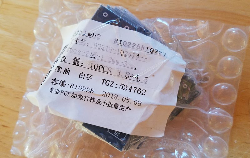
I finished the redesign for my Apple IIc Drive Switcher PCB on Monday morning, and submitted the Gerber files to Elecrow on Monday at 11:25 am. Friday at 5:20 pm I held the finished PCBs in my hands. Only 4 days for manufacturing and delivery. From China. According to the tracking info, my package took just 17 hours to travel from Elecrow’s Shenzhen facility to my doorstep in California. Total cost for everything was a mere $29.96.
We live in a crazy world, where a completely custom and intricate item can be manufactured on the other side of the planet and delivered to my door in 4 days, for the cost of a pizza and beer. Thank you Elecrow!
Read 1 comment and join the conversation10000 More DB-19 Connectors

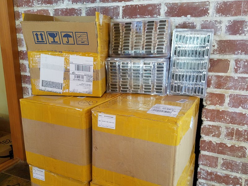
Oops, I did it again: another 10000 DB-19 connectors fresh from the factory! After helping to resurrect this rare retro-connector from the dead in 2016, and organizing a group of people to share the cost of creating new molds for manufacturing, I had some of the 21st century’s first newly-made DB-19s. The mating connector is found on vintage Apple, Atari, and NeXT computers from the 1980s and 1990s, so having a new source of DB-19s was great news for computer collectors.
But that was two years ago. After manufacturing, the lot of connectors was divided among the members of the group buy, leaving me with “only” a few thousand. Since then I’d used up more than half of my share in assembly of the Floppy Emu disk emulator, and I began to get nervous about the looming need for a re-order. It was such a big challenge the first time finding a Chinese manufacturer for the DB-19s, and the all-email company relationship was tenuous. What if they lost the molds? What if my contact there left the company? What if the company went out of business? Even though I didn’t absolutely need more DB-19 connectors until 2019 or 2020, I decided to lock in my future supply and order more now.
I needn’t have worried, and the transaction went smoothly. With no mold costs to pay this time, the only challenge was meeting the 10000 piece minimum order quantity. I was even able to pay via PayPal, instead of enduring the hassles and weird scrutiny of an international bank wire transfer like I did in 2016.
So now I have a near lifetime supply of DB-19 connectors. Call me strange, but it actually gives me a warm fuzzy feeling. Now to find someplace to store all these boxes…
Apple IIc Internal/External Drive Switcher
If you’re using a Floppy Emu disk emulator with an Apple IIc, you’ll want to see this: a switched adapter that can reassign the external 5.25 inch drive as internal, and the internal 5.25 inch drive as external. This little gizmo helps to work around the Apple IIc’s inability to boot from an externally-connected 5.25 inch drive. That shortcoming is a headache for 5.25 inch disk emulators like Floppy Emu. With this internal/external drive switcher, the limitation is now gone!
Background
The IIc has an internal built-in 5.25 inch floppy drive. The internal drive appears to the computer as slot 6, drive 1. If you connect an external 5.25 inch floppy drive, it will appear to the computer as slot 6, drive 2. Unfortunately the whole Apple II family is designed to check for a bootable disk in drive 1 only. The computer can boot from drive 1, and then use drive 2 as a secondary disk, but it can’t boot from drive 2. So for the IIc with its built-in drive 1, this means it can never boot from an external 5.25 inch drive.
An important detail: this limitation only applies to the Apple IIc with an external 5.25 inch drive. An external Smartport drive (like Floppy Emu when configured for Smartport hard disk emulation mode) appears to the computer as slot 5, drive 1, and is bootable.
Apple IIc owners who want to boot from an emulated 5.25 inch disk image are in a difficult spot. Until now, their best option has been to remove the top panel from the IIc, disconnect the internal floppy drive, and connect the Floppy Emu to the internal drive connector on the motherboard. This works fine for the Floppy Emu, but it means IIc owners forfeit their ability to use the internal drive.
How the Drive Switcher Works
There’s almost no difference between the internal drive connector on the motherboard and the external drive connector at the rear of the Apple IIc. Although they’re different shapes and even have different numbers of pins, they feature the exact same disk IO signals except one: the drive enable signal. To perform this drive switcheroo, the adapter needs to tap into the signals from the motherboard, divert the enable signal externally, and route the external enable signal back inside to the internal drive. This is easily accomplished with some headers and wires and a slide switch, but the tricky part is making it all small enough to fit inside the Apple IIc case.
A slide switch makes the drive remapping optional. At one switch position, the external drive will appear as drive 1 and the internal as drive 2. At the other switch position, the internal drive will appear as drive 1 and the external as drive 2. Now Apple IIc owners can have the best of both options.
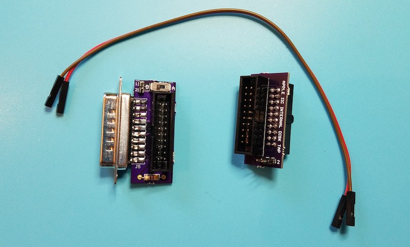
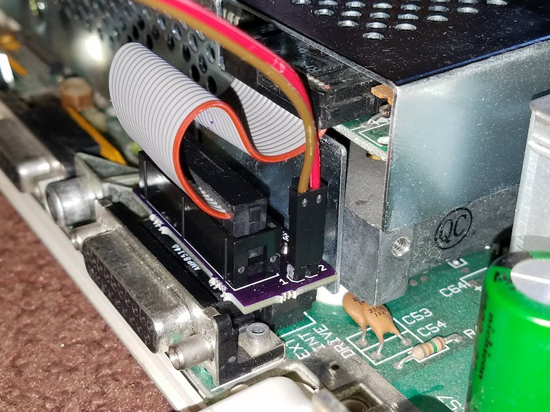
The Hardware
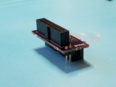
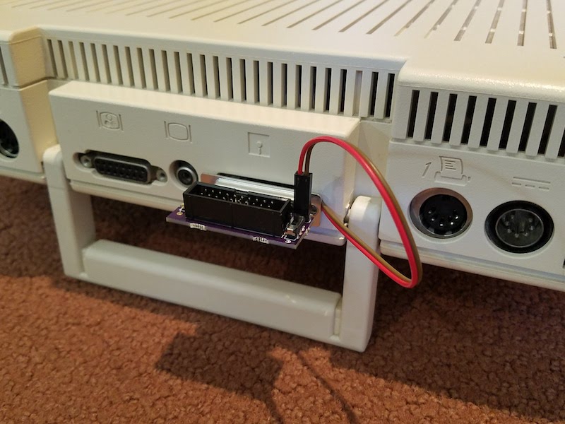
This is a two-part device: a signal tap that should be installed inside the Apple IIc, and a modified DB19 adapter with a slide switch for the external connection. Two female-female jumper wires are passed through a gap in the case to make the connection between the two parts.
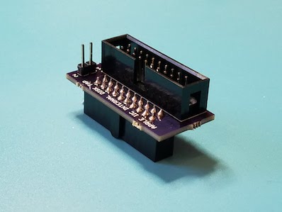
The signal tap portion of the drive switcher looks a little peculiar, and it’s a minor challenge to solder closely-spaced through-hole components to the top and bottom of a PCB like this, but it works. The top is just a standard 20-pin male shrouded header, with a polarizing key like the one used on Apple drive cables. The bottom is a PCB-mounted female version of the same connector – not a very common part, but fortunately Digikey has it. The only other component here is a 2-pin male header for attaching the jumper wires.
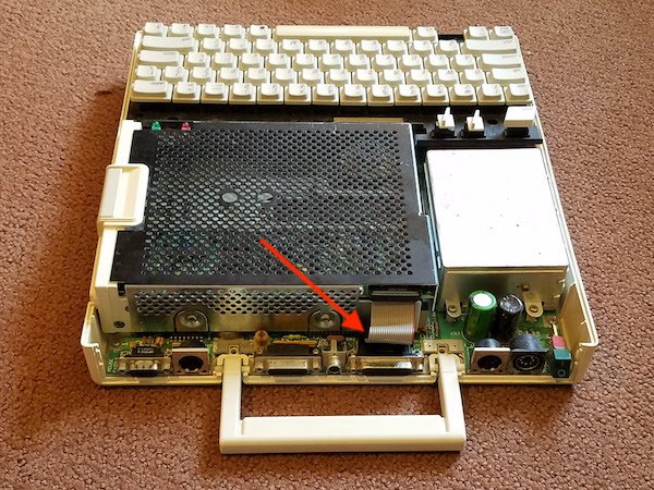
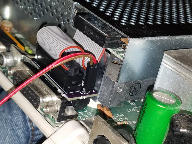
Step 1 is to remove the top panel from the Apple IIc (follow the instructions here), and locate the ribbon cable that connects the internal floppy drive to the motherboard.
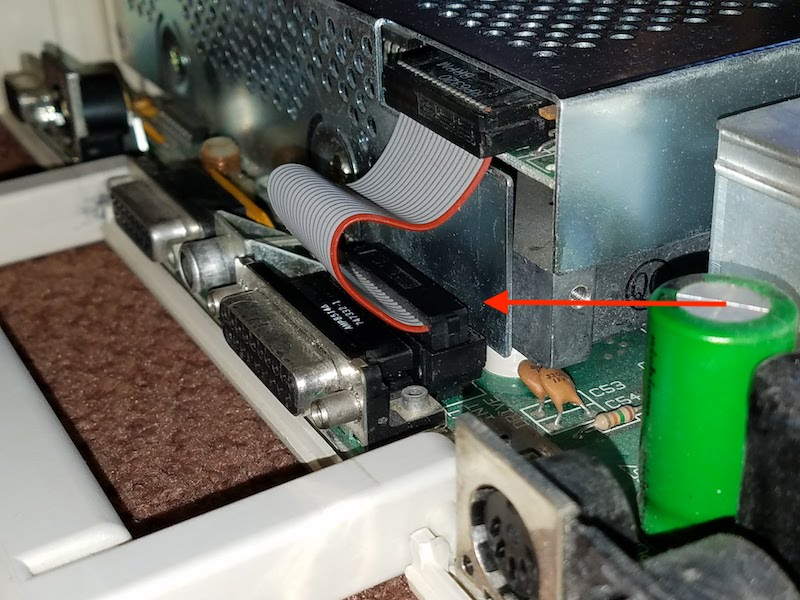
Disconnect the ribbon cable from the motherboard, and plug the signal tap into the motherboard in its place.

Then plug the ribbon cable into the signal tap. Also connect one end of each jumper wire to one of the signal tap’s male header pins. Here I chose to connect the brown wire to pin 1, and the red wire to pin 2. I’ll need to make the same choice later for the external jumper wire connections.
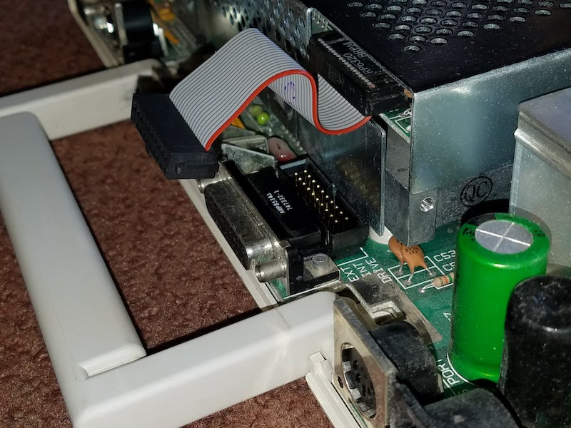
Before closing the case, it’s important to squish the ribbon cable down into the gap between the signal tap and internal floppy drive bracket. Push it down as far as it will go. This will make it easier to fit the top cover back on later. Notice the difference between the ribbon cable position in this photo as compared to the previous one:
Now it’s time to close the case. First, set the top panel loosely on the IIc, and thread the jumper wires through the opening for the disk connector in the rear of the case.
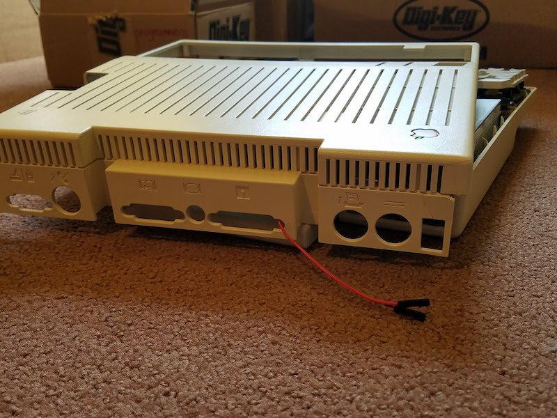
Then reinstall the top panel. It’s a snug fit, but there’s a large enough gap between the top panel and the rear connectors for the jumper wires to squeeze through. As an alternative, the jumper wires can also be threaded through the opening for the printer port or the video connector. After the top panel is reinstalled, it should look like this:
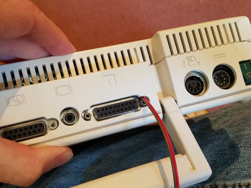
Connect the jumper wires to the 2-pin male header on the switched DB19 adapter, remembering to use the same color-to-pin mapping as before. Then plug the DB19 adapter into the Apple IIc’s external disk port. It will replace the standard DB19 adapter that’s included with the Floppy Emu.
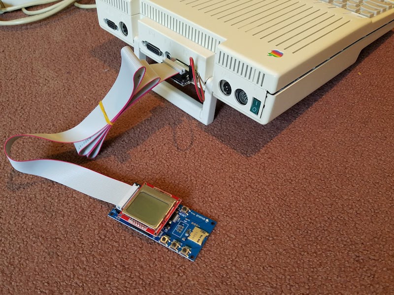
Finally, connect the Floppy Emu’s 20-pin ribbon cable to the switched DB19 adapter. All done! This Apple IIc can now boot Choplifter and other 5.25 inch disk image favorites from the Floppy Emu, while retaining the internal 5.25 inch floppy drive for secondary needs like disk copying. Or at the flick of a switch, the IIc can be restored to normal operating, with the internal floppy drive configured as the boot drive.
Coming Soon
I hope to have the IIc Internal/External Switcher ready for the BMOW store in a month or two. There are still a few wrinkles to iron out before it’s ready. Because it’s such a tight fit inside, I need to get feedback from some other IIc owners to verify the switcher fits their computers too. I also want to revise the PCB a bit, to make the switcher easier to assemble. And I’d like to provide more meaningful labels for the switch positions than simply “A” and “B”. If there were enough space, I’d label the switch positions something like “normal” and “swapped”, but the adapter is so small that there’s only room for 1 or 2 letters at most. Any great suggestions?
Read 14 comments and join the conversationInternational Shipping Struggles
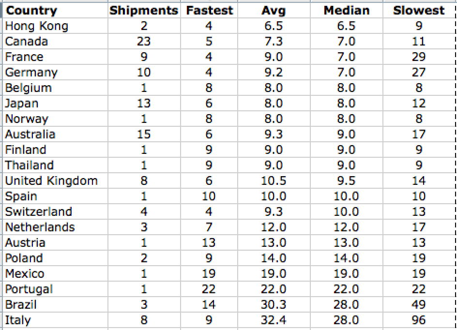
I’ve assembled some data on international shipping delivery times, for a sample of real BMOW customers over the past few months. The table shows destination countries, sorted by median delivery time. The listed time includes the shipping itself, customs inspection, and any hold time at the local destination post office waiting for the buyer to claim the package. It’s the total door-to-door delivery time. All packages are shipped via US Postal Service First Class Package International service, which is the only reasonably-priced international shipping option available to me.
As you can see, the typical delivery time varies enormously. The good news is that most countries are faster than my two-weeks generic estimate for international delivery. For the countries where BMOW has the greatest number of sales, the median delivery time is about 8 days. Poland, Mexico, and Portugal have longer delivery times, but they’re still tolerable, and I don’t have many sales in those countries anyway.
Then there’s shipping for Brazil and Italy. Ugh. Let me draw your attention to that 49-day worst case time for Brazil, and the whopping 96 DAY worst case for Italy. When a package disappears into the bowels of the postal system for 2-3 months, customers don’t blame the post office. They blame me. It’s a difficult and awkward position, and I often need to spend large amounts of time communicating with the buyer and attempting to track the package. Sometimes I have to send replacement packages or provide refunds, even though I have no control over the postal delays.
I’ve considered various ideas for the “Italy Problem”, from an express shipper option (much more expensive, and inconvenient for me), to a surcharge on orders to Italy, Brazil, and a few others (would compensate for the greater number of problem deliveries, but would be unpopular), to halting shipments to those countries completely (forcing those customers to use a 3rd-party freight forwarding service from the US).
Misrouted Packages
While collecting the data for this table, I discovered several instances where a package was sent to the wrong country, even the wrong continent! Eventually it was re-routed to the correct country, but the extra side-trip added several weeks to the delivery time. Check out these tracking histories. Follow the links and click the “Tracking History” tab:
Canadian package sent to Brazil
German package sent to Canada
French package sent to Mexico
In every case, the address on the package was correct. What appears to have happened is that the package was sent to the same country as another one of my international shipments made on the same day. I’m not sure how that could happen – surely the sorting process is automated?
Unclaimed/Refused Packages
Many countries impose an import tax or fees on merchandise purchased from another country. In such cases, typically the package will be held at the customer’s local post office, and they’ll be sent a letter informing them that the package is ready for pick-up. Then the customer will visit the local post office, pay the taxes, and claim the package.
Most local post offices will hold a package for 1 or 2 weeks. If the customer doesn’t claim the package within that time window, it will usually be returned to me. Unclaimed packages happen for a variety of reasons: the customer was away on holiday when the package arrived, or they never received the notification letter, or they forgot about it, or they declined to claim the package because they were unhappy about the taxes. Whatever the reason, unclaimed packages are always a giant pain in the ass. They usually take several months to be returned to me, if they’re returned at all. Sometimes they just disappear.
Worldwide Sales
Despite these hassles, I’ll keep selling to people everywhere, and looking for more ways to improve the international shipping experience. I’ll keep working on packaging changes to reduce shipping weight and costs, and improved labeling to speed customs inspection time. To the customers in the 42 countries where I’ve done business, thank you.
Read 6 comments and join the conversationStar Ring Version 2
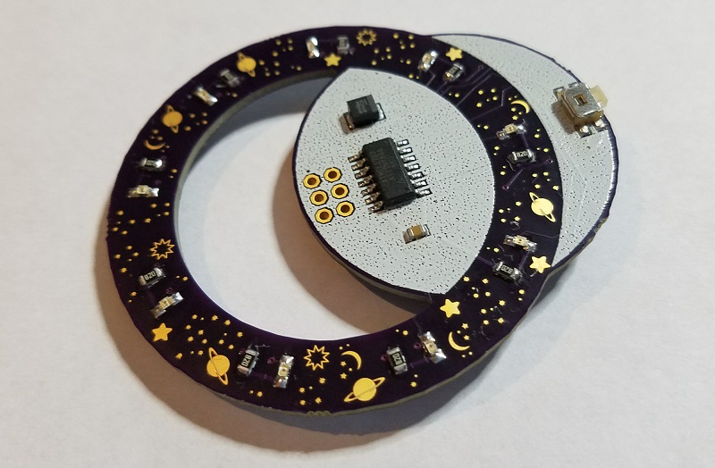
Version 2 of my PCB-abusing LED blinky is here! It’s the same odd shape as Star Ring version 1, with the same abuse of the metal layer to make shiny stars and planets, and the same low power usage and long battery life, but it adds several small improvements to function and appearance. Sure, it’s just an LED blinky, but it’s got some interesting tricks.
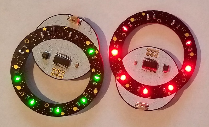
Version 2 replaces the amber yellow LEDs with either red or green. I’d imagined green would somehow be more exciting, but the red is a clear winner due to its much higher brightness. It’s not entirely obvious from the photo, but the red Star Ring has excellent brightness for something that’s driven from a puny 3V coin cell battery. The red LEDs have a 250 mcd brightness rating, as compared to 162 mcd for the amber LEDs and only 60 mcd for the green. From browsing the LED catalog, it’s clear that LED colors with longer wavelengths (closer to red) are able to achieve higher millicandela ratings at the same current and voltage. This is probably because of bandgaps and electron orbitals, or something… where’s a physicist when you need one?
Both the red and the green LEDs are 0603 sized SMD components, and they were my first-ever experience at assembling 0603 parts. Initially they seemed nearly microscopic compared to the 0805 size I use normally, and you could easily inhale one accidentally if you yawned at the wrong time, but I’m happy to report I didn’t have much difficulty with them. Each one is just 1.6 x 0.8 mm.
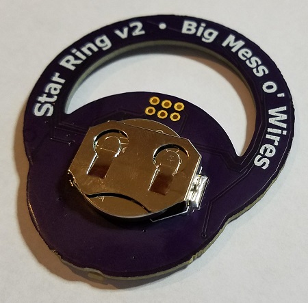
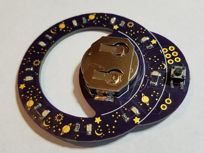
Star Ring version 1 located the battery on the front side, which was a little ugly. Version 2 moves the battery to the back, and brings the microcontroller and two capacitors to the front. It also fills the entire circular “moon” behind the star ring with white silkscreen, which really helps it to stand out visually. I think it looks great.
The tactile pushbutton was changed from a standard button to a right-angle button that’s mounted on the edge. Since it’s natural to hold the Star Ring by its edges, this makes it easy to hold the ring and push the edge-mounted button with a single hand. The version 1 Star Ring demanded two-hand operation due to its more awkward button orientation and placement.
Version 1, for comparison:
Version 3?
It would be a tight fit, but there’s probably enough room to move the microcontroller and the button to the back, along with the battery. Then the front would only have a blank white moon and the star ring itself. That might look more attractive, but it would make soldering inconvenient, so I’m not sure it would be an improvement. Keeping all the parts (except the battery) on the front makes it easy to assemble the PCB using hot plate SMD reflow.
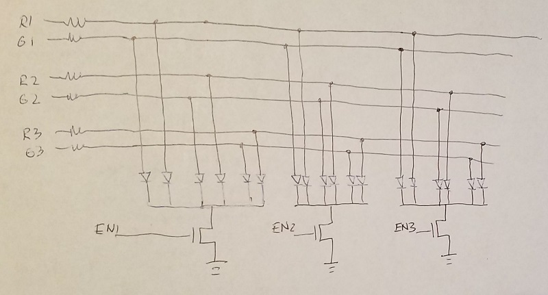
What about multi-colored LEDs? Full-color RGB is out of the question with this hardware, but what if each LED had a choice of two colors instead of being monochromatic? It’s possible to buy dual-color LEDs that are really two separate LEDs with a common cathode in a single package. A dual-color LED with red and green elements can appear red, green, or yellow depending on which of the two elements are illuminated. But dual-color LEDs would require controlling 18 LED elements instead of 9 – would I need a larger microcontroller with more IO pins? Fortunately no.
The current Star Ring hardware has 9 individually-addressable LEDs, with 9 current limiting resistors, connected to 9 IO pins of the microcontroller. The software never turns on more than three LEDs at once to avoid overwhelming the small battery, but it cycles through the LEDs so quickly that it looks as if they’re all on. Since it’s not necessary to power all the LEDs simultaneously, I worked out an alternative method where the same 9 IO pins could control 9 dual-color LEDs, organized into three groups of three dual-color LEDs each (six individual LED elements per group). Three IO pins are used to enable one of the three groups, and the other six IO pins control the six LED elements in that group. Only six current limiting resistors are required instead of nine, so even with the addition of three transistors for enabling the groups, the total component count is the same as the current design. Here’s my schematic for nine red-green dual-color LEDs:
More on Fast Interrupt Handling with Cortex M4
Can a fast microcontroller replace external glue logic, while also continuing to run application code? This is the third in a series of posts considering the question. It’s part of a potential simplification of my Floppy Emu disk emulator hardware, whose present design combines an MCU and a CPLD for glue logic. For readers that haven’t seen the first two parts, you can find them here. Read these first, including the comments discussion after the post body. Go ahead, I’ll wait.
Thoughts on Floppy Emu Redesign
Thoughts on Low Latency Interrupt Handling
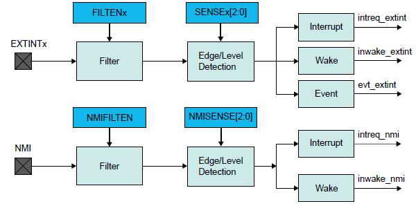
There are several pieces of CPLD glue logic that I’m hoping to replace with interrupt handlers on a Cortex M4 microcontroller, specifically the 120 MHz Atmel SAMD51 Cortex M4. The most challenging is a piece of logic that behaves like a 16:1 mux, and must respond within 500 ns to any change on its address inputs. There’s also a write function that behaves a little like a 4-bit latch, as well as some enable logic. I haven’t yet done any real hardware testing, but I’ve spent many hours reading datasheets, writing code, and examining compiler output. I’ll save you the suspense: I don’t think it’s going to work. But it’s close enough to keep it interesting.
Coding an Interrupt Handler
A 120 MHz MCU means there are 120 clock cycles per microsecond. To meet the 500 ns (half a microsecond) timing requirement for the mux logic, the MCU needs to do its work in 60 clock cycles. Cortex M4 has a built-in interrupt latency of 12 clock cycles before the interrupt handler begins to run, so that leaves just 48 clock cycles to do the actual work. At best that’s enough time for 48 instructions. In reality it will be fewer than 48, due to pipeline issues, cache misses, branches, flash memory wait states, and the fact that some instructions just inherently take more than one clock cycle. But 48 is the theoretical upper bound.
I spent a while digging through the heavily-abstracted (or should I say obfuscated) code of Atmel Start, the hardware abstraction library provided for the SAMD51. Peeling back the layers of Start, I wrote a minimal interrupt handler that directly manipulates the MCU configuration registers for maximum speed, rather than using the Start API. I ignored the write latch and the enable logic for the moment, and just wrote an interrupt handler for the 16:1 mux function. Bearing in mind this code has never been run on real hardware, here it is:
volatile uint32_t selectedDriveRegister;
volatile uint32_t driveRegisters[16];

void EIC_Handler(void)
{
	// a shared interrupt handler for changes on five different external pins:

	// EXTINT0 = PA00 = SEL - interrupt on rising or falling edge
	// EXTINT1 = PA01 = PH0 - interrupt on rising or falling edge
	// EXTINT2 = PA02 = PH1 - interrupt on rising or falling edge
	// EXTINT3 = PA03 = PH2 - interrupt on rising or falling edge
	// EXTINT4 = PA04 = PH3 - interrupt on rising edge
	// PA11 = output

	uint32_t flags = EIC->INTFLAG.reg; // a 1 bit means a change was detected on that pin

	// clear EXTINT0-4 flags, if they were set.
	EIC->INTFLAG.reg = (flags & 0x1F); // writing a 1 bit clears the interrupt flags

	// mask the 4 lowest bits and use them as the address of the desired drive register
	selectedDriveRegister = PORT->Group[GPIO_PORTA].IN.reg & 0xF;

	// don't need to check if drive is enabled.
	// output enable will be handled externally in a level shifter.
	switch (selectedDriveRegister)
	{
		case 7:
			// motor tachometer
			// enable peripheral multiplexer selection
			PORT->Group[GPIO_PORTA].PINCFG[11].bit.PMUXEN = 1;
			// choose TIMER/COUNTER1 peripheral
			PORT->Group[GPIO_PORTA].PMUX[11>>1].bit.PMUXO = MUX_PA11E_TC1_WO1;
			break;

		case 8:
			// disk data side 0
			// enable peripheral multiplexer selection
			PORT->Group[GPIO_PORTA].PINCFG[11].bit.PMUXEN = 1;
			// choose SERCOM0 peripheral
			PORT->Group[GPIO_PORTA].PMUX[11>>1].bit.PMUXO = MUX_PA11C_SERCOM0_PAD3;
			// TODO: main loop must check selectedDriveRegister to see if it's 8 or 9 when adding
			// new bytes to SPI
			break;

		case 9:
			// disk data side 1
			// enable peripheral multiplexer selection
			PORT->Group[GPIO_PORTA].PINCFG[11].bit.PMUXEN = 1;
			// choose SERCOM0 peripheral
			PORT->Group[GPIO_PORTA].PMUX[11>>1].bit.PMUXO = MUX_PA11C_SERCOM0_PAD3;
			// TODO: main loop must check selectedDriveRegister to see if it's 8 or 9 when adding
			// new bytes to SPI
			break;

		default:
			// disk state flags and configuration constants
			// disable peripheral multiplexer selection, return to standard GPIO
			PORT->Group[GPIO_PORTA].PINCFG[11].bit.PMUXEN = 0;
			// set the output pin high or low, according to the register state
			if (driveRegisters[selectedDriveRegister])
				PORT->Group[GPIO_PORTA].OUTSET.reg = (1 << 11);
			else
				PORT->Group[GPIO_PORTA].OUTCLR.reg = (1 << 11);
			// TODO: also change the PA11 output in the main loop, if the selected register
			// changes its value
			break;
	}
}
You'll notice that EXTINT4 (the PH3 signal on the disk interface) isn't actually used in this code, but it will be needed later for the write latch.
The default of the switch statement is about what you'd expect: it uses four of the inputs to construct a 4-bit address, then uses that address to access an array of 16 internal drive registers. Then it sets the output pin high or low, depending on the internal register value.
Addresses 7, 8, and 9 get special handling. These aren't really registers, but are pass-throughs of the drive motor tachometer signal or of the instantaneous read head data from the top or bottom of the disk. They're not static values, but rather are constantly changing streams of data. I plan to implement the tachometer using the timer/counter peripheral, and the read head data using the SPI peripheral. All of these functions share the same pin, PA11. The code must enable and disable the peripheral pin remapping functions as needed.
After finishing this speculative interrupt handler code, I compiled it in Atmel Studio, using gcc with -O2 optimization. Then I viewed the .lss to see what code the compiler generated:
00000c70 <EIC_Handler>:
 c70:	481f      	ldr	r0, [pc, #124]	; (cf0 <EIC_Handler+0x80>)
 c72:	4b20      	ldr	r3, [pc, #128]	; (cf4 <EIC_Handler+0x84>)
 c74:	6942      	ldr	r2, [r0, #20]
 c76:	4920      	ldr	r1, [pc, #128]	; (cf8 <EIC_Handler+0x88>)
 c78:	f002 021f 	and.w	r2, r2, #31
 c7c:	6142      	str	r2, [r0, #20]
 c7e:	6a1a      	ldr	r2, [r3, #32]
 c80:	f002 020f 	and.w	r2, r2, #15
 c84:	600a      	str	r2, [r1, #0]
 c86:	680a      	ldr	r2, [r1, #0]
 c88:	2a08      	cmp	r2, #8
 c8a:	d012      	beq.n	cb2 <EIC_Handler+0x42>
 c8c:	2a09      	cmp	r2, #9
 c8e:	d010      	beq.n	cb2 <EIC_Handler+0x42>
 c90:	2a07      	cmp	r2, #7
 c92:	f893 204b 	ldrb.w	r2, [r3, #75]	; 0x4b
 c96:	d01a      	beq.n	cce <EIC_Handler+0x5e>
 c98:	f36f 0200 	bfc	r2, #0, #1
 c9c:	f883 204b 	strb.w	r2, [r3, #75]	; 0x4b
 ca0:	4816      	ldr	r0, [pc, #88]	; (cfc <EIC_Handler+0x8c>)
 ca2:	680a      	ldr	r2, [r1, #0]
 ca4:	f850 2022 	ldr.w	r2, [r0, r2, lsl #2]
 ca8:	b9ea      	cbnz	r2, ce6 <EIC_Handler+0x76>
 caa:	f44f 6200 	mov.w	r2, #2048	; 0x800
 cae:	615a      	str	r2, [r3, #20]
 cb0:	4770      	bx	lr
 cb2:	f893 204b 	ldrb.w	r2, [r3, #75]	; 0x4b
 cb6:	f042 0201 	orr.w	r2, r2, #1
 cba:	f883 204b 	strb.w	r2, [r3, #75]	; 0x4b
 cbe:	f893 2035 	ldrb.w	r2, [r3, #53]	; 0x35
 cc2:	2102      	movs	r1, #2
 cc4:	f361 1207 	bfi	r2, r1, #4, #4
 cc8:	f883 2035 	strb.w	r2, [r3, #53]	; 0x35
 ccc:	4770      	bx	lr
 cce:	f042 0201 	orr.w	r2, r2, #1
 cd2:	f883 204b 	strb.w	r2, [r3, #75]	; 0x4b
 cd6:	f893 2035 	ldrb.w	r2, [r3, #53]	; 0x35
 cda:	2104      	movs	r1, #4
 cdc:	f361 1207 	bfi	r2, r1, #4, #4
 ce0:	f883 2035 	strb.w	r2, [r3, #53]	; 0x35
 ce4:	4770      	bx	lr
 ce6:	f44f 6200 	mov.w	r2, #2048	; 0x800
 cea:	619a      	str	r2, [r3, #24]
 cec:	4770      	bx	lr
 cee:	bf00      	nop
 cf0:	40002800 	.word	0x40002800
 cf4:	41008000 	.word	0x41008000
 cf8:	2000063c 	.word	0x2000063c
 cfc:	200005f8 	.word	0x200005f8
I don't know much about ARM assembly, but I can count 44 instructions. Already that looks pretty dubious for execution in 48 clock cycles. A couple of cache misses, or multi-cycle branches, or anything else that requires more than one clock per instruction, and the interrupt handler will be too slow to work. And if I attempt to add the missing write latch logic, the code will almost certainly be too slow. Even just an if() test to see whether the write latch was written would probably be too much extra code.
Meanwhile the microcontroller will be running the main application, responding to user input, updating the display, and streaming disk data. Occasionally the main loop will need to do an atomic operation, requiring interrupts to be disabled for a few clock cycles. If an external pin changes state during that time, the interrupt handler will be delayed by a few clock cycles.
The interrupt handler shown above is appropriate for one of the Floppy Emu's many disk emulation modes. In other modes, a different behavior is needed. A real interrupt handler would need some more if() checks at the beginning to perform different actions depending on the current emulation mode. This would add a few clock cycles more.
Even reaching this "almost fast enough" level would require some minor heroics. I'm fairly certain the interrupt handler code would need to be in RAM, not flash, to minimize or eliminate flash wait states. Even RAM might not be enough - it might need to be placed in the special "tightly coupled memory" region. The vector table itself probably also needs to be relocated from flash to RAM or TCM. This should be theoretically possible, but it's the sort of uncommon thing that's often difficult to find good documentation or examples about, and that eats up lots of development time.
To make a long story short - it doesn't look like it's going to work. And even if it did work, it might be such a pain in the ass that it negates any gain I'd get by eliminating the CPLD. And yet it looks pretty close to working, at least within a factor of two if not less. If the timing requirement were 1000 ns instead of 500 ns, I think I could make it work.
Other Interrupt Oddities
According to the docs I've read, interrupt handlers on ARM are just like any other function. There's no special interrupt prologue or epilogue, and there's no RTI return from interrupt instruction. And yet gcc does specify an interrupt attribute for ARM functions:
__attribute__ ((interrupt))
The code in Atmel Start doesn't appear to use that attribute for its interrupt handlers. So is it needed or not? What does it do? As best as I can tell, it adds some extra code that aligns the stack pointer upon entry to the interrupt handler, but why? If I add the interrupt attribute to my EIC_Handler(), it gets many instructions longer.
Another unanswered question is how to handle nested interrupts. EIC_Handler wouldn't be the only interrupt handler in the firmware, but it should be the highest priority. If another interrupt handler is running when an external pin changes state, that handler should be pre-empted and EIC_Handler should be started. The Cortex M4 supports nested interrupts, but is there any extra code needed in the interrupt handlers to make it work correctly? Extra registers that must be pushed and popped? I'm not sure, but this discussion suggests the answer is yes. If so, that would add still more instructions to the interrupt handler, making it even slower.
Read 15 comments and join the conversation