

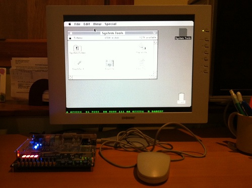
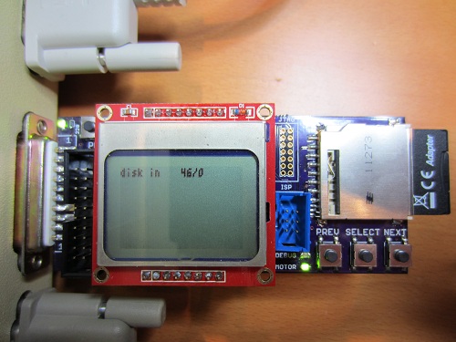
Floppy Emu Disk Menu
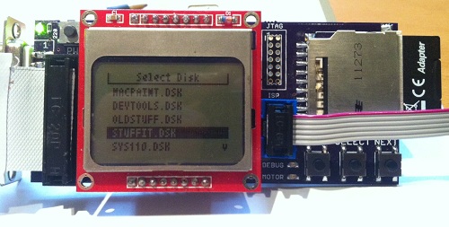
I finally got around to building a proper floppy disk image selection menu. Instead of loading a hard-coded rfloppy.dsk disk image file from the SD card, Floppy Emu now scans the SD card for all files with a .dsk extension, and displays a menu of available disk image files. The PREV/NEXT buttons navigate the menu, and the SELECT button inserts the selected disk image into the virtual floppy drive.
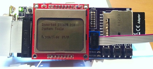
When a disk image is inserted, the LCD displays the name of the Macintosh volume that’s inside the disk image – “System Tools” in the example above. It also shows the current track and side being accessed. For write operations, the LCD displays the track, side, and sector that was written, as well as the time required for the write.
Download the Floppy Emu file archive for the new firmware.
Be the first to comment!
Plus Too Files
Since the Plus Too project hasn’t seen any progress in a year, I’m posting all the design files in the hopes that someone else may want to build on what I’ve done. If you missed the earlier discussions about it, Plus Too is a working replica of a Macintosh Plus, implemented in an FPGA.
Download the Plus Too file archive
What You’ll Need
- An Altera DE1 FPGA development board
- A Windows-based PC
- An old PS/2 mouse from a PC (newer USB-based mice won’t work)
- A VGA monitor capable of displaying 1024 x 768 @ 60Hz
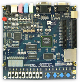
Setup Instructions
- Download the Control Panel configuration file DE1_USB_API.sof into the FPGA. This file is included on the CD that comes with the DE1 kit. See sections 3.1 and 4.1 of the DE1 user manual for help.
- Run the DE1_Control_Panel.exe program on your PC. This is also included on the DE1 CD.
- Click on the Flash tab.
- Click the Chip Erase button to clear the DE1 Flash memory.
- In the Sequential Write section, enter 0 for the address and click the File Length checkbox.
- Click the Write a File to Flash button. When prompted, select the plusrom.bin file from the Plus Too archive, and write the file to the DE1 memory. This is a ROM dump from Macintosh Plus.
- In the Sequential Write section, enter 20000 (hex) for the address. Confirm the File Length checkbox is still checked.
- Click the Write a File to Flash button. When prompted, select the Disk608-800K.bin file from the Plus Too archive, and write the file to the DE1 memory. This is a System 6.0.8 boot disk image.
- Download the Plus Too configuration file plusToo_top.sof into the FPGA. This is included in the Plus Too archive.
You should now be up and running! Connect a PS/2 mouse and a VGA monitor for some retro-computing fun.
Using Plus Too
There’s no support for the keyboard, sound, or SCSI. The floppy disk is read-only.
Watch out! There’s a bug somewhere that causes PlusToo to crash or the mouse to stop working (not sure which) if you move the mouse around too much or too fast. I’m still not sure what the cause is, but I wrote about it more in a previous post.
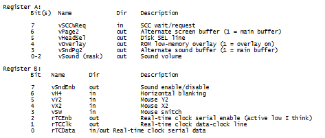
Along the bottom of the screen you’ll see some debug information, shown in green text. From left to right, these are:
- A – the current value on the address bus
- D1 – the incoming value from the data bus
- D0 – the outgoing value from the data bus
- (not labeled) – the current interrupt level
- AA – the previous value of the address bus
- B – the breakpoint address
You can set the breakpoint address using the DE1 switches. When the current address equals the breakpoint address, Plus Too will halt.
The hardware can be controlled using the four push-button switches on the DE1 board, which are labeled Key0 through Key3, as well as the 10 slide switches labeled SW0 through SW9.
- Key2 inserts a blank disk into the external drive. Useful for debugging only.
- Key1 inserts the System 6.0.8 disk into the internal drive.
- Key0+Key1 together perform a reset.
- SW0 selects between free-running (switch down) and single-step mode (switch up).
- When in single-step mode:
- Key0 performs a step
- Key1, Key2, and Key3 load the low, middle, and high bytes of the breakpoint address from switches SW9-SW2.
Making Floppy Disk Images
The Disk608-800.bin file is not a standard floppy disk image file such as you would use with a Mac emulator like Mini vMac or Basilisk II. It’s an encoded file containing data exactly as it would appear on a real floppy disk, complete with sector markers, checksums, and inter-sector timing gaps.
If you want to take an 800K floppy image from your favorite emulator and use it with Plus Too, you’ll need to encode it using my Floppy Encoder utility. It takes a normal floppy image file as input, which usually has a .dsk filename extension, and generates an encoded image file with a .bin extension. The resulting .bin file can then be substituted in step 8 of the setup instructions to run Plus Too with the new floppy image.
Extending Plus Too
The Verilog source files are included in the file archive, for anyone who wants to try taking the project further. The biggest thing it needs now is for someone to set up proper timing constraints. I played around with it a bit, but I didn’t really understand the constraint editor and was eager to move on. PlusToo mostly works without specifying any constraints, but sometimes it will randomly fail to boot up, or exhibit bizarre video bugs. I’ve found that changing the number of signals and sample depth of the Signal Tap logic analyzer setup can fairly predictably make such problems appear and disappear.
The constraints should be:
- External 50 MHz clock
- Internal 32.5 MHz clock synthesized with a PLL. This is the video clock, called clk32 in the Verilog source.
- Internal 8.125 MHz clock named clk8, derived from clk32 with a clock divider. (I couldn’t make this work with a PLL)
- Flash ROM has an address-to-data delay of 70ns. The total delay from clk8 to when all the Flash control and address lines are stable, plus 70 ns, plus whatever the setup time is for the FPGA registers that will receive the Flash data (how do you determine this?), must be less than the clock period of 123ns.
- Similarly for the SRAM, except I believe its address-to-data delay is 10ns (check datasheet). The SRAM should also have additional constraints for write timing.
Read 23 comments and join the conversation
Tranz 330 Files
 I’ve posted an archive containing the original Tranz 330 program file dump, my commented disassembly of the original program, and two versions of the Mozart demo in source and binary form. If you can get your hands on a Tranz 330 from a surplus electronics supplier, this should give you an afternoon’s entertainment! You can grab the files here.
A New Kind of Video Game Console

A few months ago I posted a long essay on my professional future. Should I try to make a career of BMOW blogging? Find an electronics industry job? Return to video game development? Launch a start-up company? Since then I’ve been engaged in many parallel paths, trying to do all those things at once. I’ve drafted business plans, pitched to Sand Hill Road venture capitalists, taken countless coffee meetings with angel investors, rubbed elbows at meet-ups, and generally abused my network of friends, their friends, and their friends’ friends for any worthwhile leads on interesting opportunities. It’s been a crazy, exciting, and confusing time.
I’m happy to say that all those parallel paths have finally converged, and this week I joined Kickstarter wonderkid OUYA as Head of Engineering! It’s software + hardware + games, and I could hardly imagine a better opportunity. OUYA is a $99 video game console, based on the Android OS, where all the games are free downloads. By removing the roadblocks associated with traditional console development, it opens up the TV as a platform to smaller indie developers for the first time. Every OUYA console is also a dev kit, so there’s nothing more to buy. It’s built on Android, so developers already know how it works. Gamers benefit from increased variety and the ability to try any game in the OUYA catalog before purchasing additional in-game content. Hackers are welcome, and rooting won’t void your warranty.
The hardware is based on the Tegra 3 SoC, which combines a quad-core ARM processor with an nVidia GeForce GPU. This is the same chip used in Android tablets like the Google Nexus 7 and Asus Transformer Prime. Those who don’t follow mobile technology closely will be amazed at how powerful this hardware is. Placed in a game console with HDMI output, and freed from concerns about battery life, the Tegra 3 can compete on the level of the Playstation 3 and XBox 360. The bluetooth controller combines analog sticks, buttons, and a touchpad, and boasts a beautiful industrial design from fuseproject’s Yves Behar.
OUYA launched its Kickstarter campaign earlier this summer, and blew past its funding goal within the first few hours, eventually raising more than $8 million in pledges and pre-orders. The response from both gamers and developers has been overwhelming. Clearly the OUYA concept has struck a chord within the community. There’s been some understandable skepticism about OUYA in the press, suggesting it’s a group of well-meaning amateurs with no hope of actually delivering on its promises. But after digging into the details myself and getting to know the leaders of the company, I can tell you nothing could be further from the truth. I’m confident in betting my own future on its success.
This is a hardware blog, so I need to emphasize that I’ll be running the software development part of OUYA’s business. The hardware development is in the capable hands of Muffi Ghadiali, a veteran of past consumer electronics projects such as the Kindle Fire and HP TouchSmart computer. nVidia and its Asian manufacutering partners are also a huge source of assistance. So I won’t be breaking out my soldering iron at the office, but my background in electronics means that I can work effectively with the hardware team. And I get to geek out with pre-release hw prototypes!
My task is to finish development of the OUYA SDK, the console’s browser/store interface, the developer portal web site, the payment system, and all the other technology that’s needed for the March 2013 launch. I’ll be doing all this with a team operating from a satellite office in the San Francisco Bay Area (marketing, sales, and OUYA’s corporate office are in Los Angeles). This is much the same kind of work I’ve done in the past at Trion Worlds and Electronic Arts. At Trion we built the MMO RIFT, which was a great experience in leading a team to build a complex online service from scratch. And at EA I created many console games for the Playstation, XBox, and other systems, and I know what a pain it is to deal with the balky dev kits, tools, and mind-numbing technical requirements. I’m thrilled to be introducing a new kind of video game console that will open up the TV platform like never before.
Read 7 comments and join the conversation
Finally!
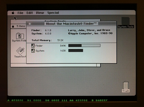
The new Floppy Emu prototype is up and running at last! Today I was able to boot a Mac Plus from the new emulator board for the first time. It’s still rough around the edges, but it works. Copy a Macintosh disk image to your SD memory card, then plug the Floppy Emu board into your Mac’s external floppy port, and presto: instant disk drive. Your vintage Mac never even knows it’s not the real thing, so everything runs just like it would with a real external floppy drive.
It’s hard to believe it was nearly five months ago that I set out to replace my first ball-of-wires breadboard prototype with something better. The changes seemed simple enough: switch to a more powerful microcontroller from the same family, substitute a different brand of CPLD, add a few more buttons and connectors, and mount the whole thing on a small circuit board. But then I let the project gather dust for a few months, and when I returned to it, almost everything that could possibly go wrong did. Seemingly minor changes to clock speeds and interrupt configurations led to all kinds of head-scratching failures. They’re not interesting enough to detail, but you can imagine a string of long evenings filled with me pounding my fist on the desk and shouting rude things at the monitor.
One of the coolest features of the new board is that the microcontroller can program the CPLD via JTAG, using the XSVF player code that I discussed in my previous post. Copy a firmware.xvf file to the SD card, reset the Floppy Emu board while holding down both PREV and NEXT, and the CPLD will be updated with new firmware in about 20 seconds. That means an external Xilinx programmer isn’t needed at all, which is a huge win. I hope to later implement bootloading of the microcontroller from the SD card too. If I ever reach the point of selling assembled units, that means end users could update both the CPLD and the MCU just by copying the necessary files to the SD card, without any programming hardware at all.
There’s still a lot left to do. I haven’t yet tested write emulation with the new prototype, so that’s the first task. It should work, but it took me so long to get read emulation working that I wanted to savor the success for a while before enabling and testing the write emulation code. Then I’ll look at some new buffering schemes for write emulation, using the extra RAM found in the ATMEGA1284P microcontroller that the new prototype uses. That should hopefully make write emulation more reliable than in the first prototype. At some point, I also need to add support for 400K and 1.4MB floppies, since the current emulator is 800K only.
The user interface needs improvement too. I’d like to add a nicer way to trigger CPLD programming, and a menu to select from among many disk images on the SD card. It would also be nice to add features like an auto-insert option, to insert a particular floppy image into the virtual drive immediately when Floppy Emu is first powered on.
Two features that you probably won’t see are emulation of more than one floppy drive at a time, and emulation of disks larger than 800K (or 1.4MB on those machines that support it). Those limitations come from the Macintosh floppy driver code in ROM, so to change them I’d need to write a new driver, and find a way to load it using the built-in driver so that the new driver replaces the built-in driver after loading. In fact, I’d probably need to write a new driver for every Macintosh model, since they don’t all access the floppy hardware the same way. It’s all theoretically possible, but would be a major software project that I’d prefer to leave to someone else to attempt.
To my friend Tom who keeps hounding me asking when Floppy Emu will be ready, here you go. Your Mac 512K can now live again!
Read 16 comments and join the conversation
In-System CPLD Programming Using XSVF Files
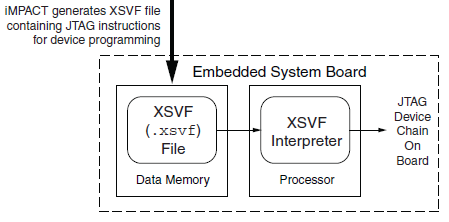
Floppy Emu has both a microcontroller and a CPLD working in tandem, and both must be programmed in order for the emulator to function. However, I don’t want to require two separate external programmers and the associated port connectors. My plan is to use a standard external ISP programmer for the microcontroller, but have the microcontroller program the CPLD, using the technique described in Xilinx app note XAPP058. The idea is to have the microcontroller act as an XSVF player, loading the CPLD configuration file from the SD memory card, and bit-banging the four JTAG pins on the CPLD to perform the programming.
This week, I finally got around to working on the XSVF player so I could program the CPLD on the Floppy Emu prototype board. The Xilinx player sample code is written in C, and was fairly easy to integrate into the emulator program. Using the functions I’d previously implemented, it was quick work to add an option to load a config file from the card and execute it with the XSVF player.
Predictably, once all the pieces were in place, it didn’t work. I spent a while checking and re-checking all my assumptions, reviewing the code, and writing debug info to the LCD, but made no progress. Finally I used the oscilloscope to peek at the JTAG signals, and discovered that they weren’t wiggling at all. All four JTAG signals were stuck high. I spent a few more hours chasing various theories why that might happen, and double-checked the electrical connectivity, before I gave up to do something else. Immediately after leaving the room, I suddenly realized what the problem was: in order to programmatically control the microcontroller JTAG pins, the JTAGEN fuse must be turned off, to disable hardware JTAG. Once I did that, the signals began wiggling as expected when I ran the XSVF player.
At this point the outgoing TMS, TCK, and TDI signals looked reasonable, but the JTAG communication still didn’t work. The error code from the player indicated that the TDO data returned from the CPLD didn’t match what was expected. Again the scope proved useful, this time by showing that TDO was stuck low, and never changed its value. No wonder the data didn’t match what was expected– it was always zero.
Here’s where I would normally describe how I finally solved the problem and got everything working, except this time I didn’t. At this moment TDO is still stuck low, and CPLD programming or other JTAG communication is not possible. I’ve examined the TMS, TCK, and TDI signals, and they look reasonable, and appear to roughly match the output of the PC-based XSVF player simulator that’s part of the Xilinx sample. So what might be wrong? Some theories, none of them great:
- The CPLD’s JTAG controller might not be active. But according to the datasheet, “If the device is in the erased state (before any user pattern is programmed), … the JTAG pins are enabled to allow the device to be programmed at any time. All devices are shipped in the erased state from the factory.”
- The JTAG controller might be in the wrong state to respond to the commands from the XSVF player. However, I looked at the code, and the first thing it does is reset the controller (by setting TMS high and pulsing TCK five times). This should be OK.
- The communication from the XSVF player might be garbled or broken. Maybe I accidentally swapped two signals, or introduced a bug in the player code? My preliminary scope debugging shows the signals look OK, so I’m skeptical this is the problem.
- The JTAG clock might be too fast. Initially the player code resulted in a JTAG clock rate around 500 kHz. I tried slowing it to under 1 KHz with no success.
- The player might not be waiting long enough for CPLD internal operations to complete. There’s a fairly long discussion of this in the sample code, and I’m fairly sure I did it correctly. When I tried slowing down the player even further, it didn’t help.
- The XSVF file might be bad. I’m using a file I generated with Xilinx iMPACT, which should simply query the device ID, then terminate.
- There might be an electrical short between TDO and ground. I’m fairly certain this isn’t the case, because before I disabled microcontroller’s JTAGEN fuse, TDO was about 4.5 volts. Now it’s zero. If there were a short to ground, it would have always been zero.
- The CPLD might be installed backwards or rotated, so the board trace isn’t actually connected to the TDO pin. I double-checked the orientation, and it looks correct.
- The CPLD might be damaged or defective.
For the moment at least, I’m stumped. I’m out of ideas for other things to try. I’m going to set this aside for a while, and hope that the solution will suddenly occur to me while I’m working on something else. Or failing that, I may at least come up with new theories that can be tested. Debugging electronics sure can be a pain!
Read 8 comments and join the conversation