

Plus Too Video and Audio
I’ve been working through the details of the video and audio systems for my “Plus Too” Mac Plus clone, and things are beginning to fall into place. Here’s what I’m planning:
Video
The Plus Too will have a VGA output for connection to a standard monitor. The video will be monochrome 1024 x 768 at 60 Hz, containing a pixel-doubled image of the Mac’s 512 x 342 frame buffer. The doubled image will fit perfectly across the horizontal, but there will be some letter-boxing vertically since 2 times 342 is less than 768.
Because the pixel clock, CPU clock, and audio sample rate in the Mac are intimately related, the choice of 1024 x 768 60 Hz video will affect the possible CPU and audio rates. The 1024 x 768 @ 60 Hz VGA standard requires a pixel clock of 65 MHz. But because the image is pixel-doubled from a 512-pixel wide original, and not a true 1024-pixel image, the effective pixel clock is only 32.5 MHz. The original Mac had a 2:1 ratio of pixel clock to CPU clock, which was a result of the 16-bit memory bus width and the 50/50 time sharing of RAM between the CPU and video circuitry. Assuming the same 2:1 ratio, that would give the Plus Too a CPU clock speed of 16.25 MHz. That’s twice as fast as the original Mac, and not so good for building a faithful reproduction of the original. Unfortunately the CPU clock speed can’t be changed independently of the pixel clock without changing either the bus width or the memory interleaving scheme.
My solution is to run the CPU at 8.125 MHz, but “double pump” the RAM during each turn of the video circuitry, fetching 32 bits per turn instead of 16. This is possible because each turn is 4 CPU clocks long, which in 1984 was only long enough for one RAM access, but in 2011 is certainly long enough for two accesses, given modern SRAM speeds. Two 16-bit reads per turn will fetch 32 pixels worth of data. With a video turn occurring every 8 CPU clocks, that’s a turn rate of 8.125 / 8 = 1.016 MHz. 32 pixels at a rate of 1.016 MHz yields the required pixel clock of 32.5 MHz. Thus the Plus Too will have a 4:1 ratio of pixel clock to CPU clock.
8.125 MHz is still about 4% faster than the 7.8336 MHz CPU of the original Mac Plus (and 128K and 512K). But it’s close enough that the discrepancy shouldn’t be very noticeable.
Audio
Including the VBLANK region, the original Mac had 370 lines of video per frame. The audio hardware had a 370 byte sample buffer, and it’s not a coincidence that those numbers are the same. At the end of every horizontal video line, the hardware fetched a single byte from RAM and used it to update the audio DAC (which was not actually a DAC, but ignore that for a moment). Since the horizontal line rate was 22.2 kHz, this provided 8-bit 22.2 kHz audio. The contents of the audio buffer were played (output to the speaker) exactly once per frame.
Since the Plus Too hardware won’t have 370 lines of video per frame, having a 370 byte audio buffer is problematic. Ideally I could change the size of the audio buffer to match the new number of lines per frame, which is 1334 lines (including the VBLANK region) for my chosen video mode. Sadly, that 370 number is embedded in the Mac’s memory map and sound routines, and realistically can’t be changed. I see three possible ways to address this:
- Read a byte and update the audio DAC after every four lines of video. That would be 1334 / 4 = 333 bytes per frame, resulting in a playback rate of 20 kHz — about 10% too slow. The slowness probably wouldn’t be too noticeable. The bigger problem would be that the entire sound buffer wouldn’t be played during a single frame. Frame-synchronized code that filled the sound buffer with the next 370 bytes of data during the VBLAK interrupt would no longer work as intended. Audio would sound oddly distorted.
- Abandon the relationship between video lines and audio samples, and just divide the frame’s time into 370 intervals, fetching audio bytes at equal intervals. This might result in an audio fetch being attempted when a video fetch or CPU memory access was happening. The audio fetch would need to be delayed until the next CPU turn, and then steal the CPU turn, forcing the CPU to wait further. With some more complicated logic for /DTACK generation to force CPU wait states, this could probably work.
- Change the address decoding scheme to map the audio buffer into a 370-byte dual-port buffer implemented within the FPGA itself. Then read 370 samples per frame from the buffer at equal intervals, as with option #2. The advantage here is that the /DTACK generation circuit wouldn’t need to change and the CPU wouldn’t be forced to wait. The dual-port buffer would make it possible for the CPU to write simultaneously with an audio hardware fetch. 370 bytes isn’t very much (most FPGAs have 10K or more embedded RAM), so this might be the easiest solution.
I spent quite a bit of time considering these three options, until I realized that I could experiment with all three simply by reprogramming the FPGA after the hardware is built. The physical hardware on the board would be identical in all three cases, so I can defer a final decision until later.
Returning to the issue of the it’s-not-a-DAC, the final question is the design of the audio output circuit. The original Mac used PWM to generate the audio signal, with the amount of time that the line was high determined by the most recent audio byte. A filtering circuit smoothed this high-speed PWM signal into an audio frequency, and attenuated it to one of eight volume levels using a 3-bit volume control. The exact circuit is here (drawn by 68kmla.org forum member H3NRY):
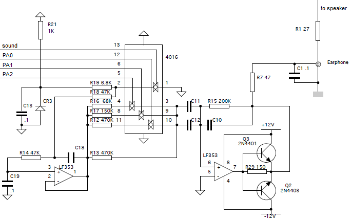
Uh… what? I see the PWM signal and 3-bit volume control coming in from the left, but everything else is lost in a sea of capacitors, diodes, op-amps, and transistors. I’m no analog guy, and I really don’t understand how this circuit works– especially the part where an op-amp drives the base of two transistors. I could just build this circuit as drawn, without understanding it, but I’d prefer to create my own solution even if the resulting audio quality is inferior. From examining this schematic, I’m unsure how much attenuation each bit of the audio volume is supposed to produce, but I could probably measure that experimentally from a real Mac Plus, or just make up some values that work well subjectively. There are a few Arduino how-tos for PWM audio that could serve as a starting point, or I could simply use a real hardware DAC.
Read 9 comments and join the conversation
68000 Interleaved Memory Controller Design
Continuing my efforts on the Plus Too Macintosh Plus clone, I’ve started work on the design of the interleaved memory controller. The memory controller allows RAM to be transparently shared between the 68000 CPU and the video circuitry. The general principle of operation is clear, and is described in many articles about the Mac 128K/512K/Plus, as well as discussions of machines like the Amiga and Atari ST that used a similar scheme. The memory controller forces the CPU and video circuitry to take turns accessing the RAM’s address and data busses. The video circuitry is designed to guarantee that it only accesses RAM during its turn. If the CPU attempts to access RAM out of turn, the memory controller forces it to wait.
I’ve tried to find specific implementation details for this scheme, or a circuit schematic of the memory controller for the Mac, but came up empty-handed. Instead I’ll make some educated guesses about how it worked on the 128K/512K/Plus, and design the circuit myself.
CPU Wait
My first unanswered question is the method used to stall the 68000 if it attempts an out-of-turn RAM access. It’s possible the Mac Plus memory controller gated the CPU clock to stall it when needed, or used the /HALT line. It’s also possible that it used the bus request and bus grant lines /BR and /BG to request the bus from the CPU. However, it’s more likely that it used the 68000 /DTACK line to insert CPU wait states, since this is essentially what that line is for. Some discussions of the Amiga memory controller mention that it used /DTACK for a similar purpose, and it seems reasonable that the Mac did too. During a memory bus cycle, the 68000 expects /DTACK to be asserted by the memory to acknowledge a read or write operation, and it waits as long as necessary until receiving that acknowledgement.
Memory Interleave Pattern
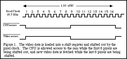
My next question is the exact pattern of interleaved access, and the fraction of time dedicated to the CPU vs the video circuitry. Details are very hard to come by, but it appears that the Plus shared 50/50 between the CPU and video circuitry, with four clock cycles of CPU access followed by four clock cycles of video access. This article at MacTech was the only reference I found, although it shows 16MHz pixel clock cycles instead of 8MHz CPU clock cycles. Here’s their diagram:
Interestingly, the Mac SE seems to have used a 75/25 split, with the CPU having access to RAM 75% of the time, accounting for the SE’s performance edge over the Plus. The Atari ST and Amiga appear to have both used a more aggressive scheme where video circuitry access occurred during known dead time in the 68000 bus cycle, so the CPU never had to wait. This would have required the use of higher speed RAM than found on the Plus or SE, in order to squeeze the video memory access into that timing window. Again, hard details on the memory controller for any of these machines is difficult to find, and this is my interpretation of the many vaguely-worded descriptions I found.
While I could get better performance from my Mac clone by using the ST/Amiga technique, I will use the slower Plus technique to make the clone’s behavior as similar as possible to a real Plus.
68000 Bus Cycle Timing
To really understand how the memory controller can work, it’s necessary to study the 68000 bus cycle timing. The most important point is that all 68000 memory accesses require at least 4 clock cycles. Assuming fast enough memory, they will never require more than 4 clock cycles, so 4 clocks per memory access is the norm. When I first discovered this, I was a bit shocked, since it embeds the “CPU is much faster than RAM” concept directly into the CPU’s design. Even if the RAM were fast enough to perform a read or write in a single clock cycle, the 68000 will still take 4 clock cycles to perform the memory operation. These 4 clock cycles are divided into 8 states named S0 to S7, each half a cycle in length. Here’s a diagram from the 68000 datasheet:
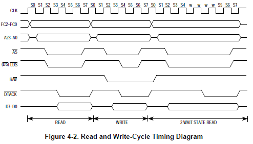
The 68000 sets up the address, strobe, R/W, and data lines (for a write) during states S0 to S3, and expects /DTACK to be asserted at the end of S4. If it’s not, it inserts wait states until /DTACK is asserted, at which point it advances to states S5-S7 to complete the bus cycle. Data is actually latched at the end of S6, and the address and strobe lines are deasserted in S7, to prepare for the next bus cycle.
Memory Controller Design
Note that the 68000’s TAS (test and set) instruction uses a unique 10-clock (20 state) bus cycle that doesn’t fit this pattern. Therefore TAS won’t work using this memory controller. I strongly suspect it didn’t work on the Mac Plus either.
With the 4-clock bus cycle pattern, the necessary structure of a memory controller begins to get clearer. The core is a circuit that delays the assertion of /DTACK if the CPU attempts an out-of-turn RAM access. It also needs a 3-bit counter to count 8 clock cycles and keep track of whose turn it is: the MSB of the counter can serve as the “turn bit”, providing 4 clock cycles each to the CPU and video. A bidirectional bus driver (74XX245 equivalent) will be needed to isolate the CPU and RAM data busses, connecting them only during the CPU’s turn. And a mux will be needed to select between the CPU address and video circuitry address, providing one or the other to RAM depending on the turn bit.
The final detail is the phase relationship between the 3-bit clock counter, and the 68000 bus cycle. If new bus cycles always start when the counter value is 0, then everything will work fine, and the turn bit will change state exactly at the beginning and end of a CPU bus cycle. If they are out of phase, however, bad things could happen, because the turn bit could change in the middle of a bus cycle. This would cause a CPU write to fail, or a CPU read to retrieve garbage. Clearly, some mechanism must force the CPU bus cycles to stay in phase with the cycle counter. There’s some cryptic “read phase” code in the Mac ROM that’s executed very early during the boot process, which I’m sure is related, but damned if I can figure out what it does. There’s a mention of it in this discussion of the Mac 128K.
Putting this all together, here’s my design for a 68000 system containing RAM and ROM and using an interleaved memory controller to share RAM between the CPU and video circuitry. Glorious diagrams courtesy of MS Paint.
First, consider the ROM. Because the CPU is the only component that accesses ROM, the CPU address and data busses can be connected directly to the ROM. All that’s needed is an address decoder to determine whether the current CPU address maps to somewhere in ROM, and generate the ROM chip select signal. A valid memory access will be detected when /AS and one or both of /UDS and /LDS are asserted. This /VALID signal can be connected directly to /DTACK, so the CPU indirectly generates the acknowledge signal itself.
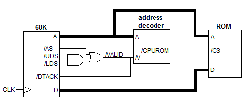
For simplicity this ignores the CPU’s R/W line, and will cause bus contention if you attempt to write to ROM, but the /DTACK behavior is easy to understand.
Now add RAM to the system, along with a linear address generator for video, a video shift register, and other hardware necessary to make it all play nicely together:
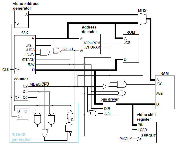
Holy cow, what’s going on here? The CPU address and data busses are still connected directly to the ROM, so that hasn’t changed. /DTACK is now generatred by a more complex circuit outlined in blue, which I’ll return to in a moment.
A three bit counter is incremented every clock cycle, counting a pattern of 8 cycles. When the counter’s MSB Q2 is 0, the CPU may access the RAM, but when Q2 is 1, the video circuitry accesses the RAM and the CPU can’t. A mux selects between the CPU address and video address using Q2 as the selector, with the selected address provided to the RAM. The CPU data bus is isolated from the the RAM’s data lines using a bidirectional bus driver. The bus driver is enabled only when Q2 is 0 and /CPURAM is asserted, meaning it’s the CPU’s turn to access the RAM and RAM is in fact being accessed. The direction of the bus driver is controlled by the CPU’s R/W line.
The RAM is selected whenever Q2 is 1 (it’s the video circuitry’s turn) or /CPURAM is asserted. This means the only time the RAM won’t be selected is when it’s the CPU’s turn, but it’s accessing another memory or peripheral instead of the RAM. The RAM is enabled for writes when it’s the CPU’s turn, /CPURAM is asserted, and the R/W line is 0.
When it’s the video circuitry’s turn, a 16-bit data word from the RAM is loaded into the parallel input of the video shift register. Pixel data for a 1-bit display image is then shifted out the serial output, 1 bit per pixel clock. The pixel clock runs at twice the system clock frequency, and 16 pixels are sent to the display during the 8 system clocks of the three bit counter.
That brings us to the /DTACK generation circuit, which implements the equation:
/DTACK = /VALID + //CPURAM * (/Q2*/Q1 + Q2 + /Q2*Q1*Q0*//LASTDTACK)
Where // indicates negation of a negative logic signal.
So what the heck does that do? Let’s break it down. Whenever this equation results in a value of 1, it means /DTACK will not be asserted, and if the CPU is in state S4 waiting for /DTACK, it will enter a wait state. The equation shows that /DTACK will not be asserted if:
- /VALID is not asserted – No valid address, no acknowledgement. Makes sense.
- Or the CPU is attempting to access the RAM, and any of the following are true:
- Counter value is 0 or 1, indicating the CPU is supposed to be in bus cycle states S0 through S3.
- Counter value is 4 or greater, indicating it’s the video circuitry’s turn, not the CPU’s.
- Counter value is 3 (bus cycle states S6 or S7) and /DTACK was not asserted during the previous clock (bus cycle states S4 and S5)
In the case where the CPU is accessing ROM or another peripheral, the second OR clause drops out, and /DTACK = /VALID as in the earlier ROM-only example. Otherwise /DTACK will be asserted only during the CPU’s turn when the counter equals 2 (CPU should be in bus cycle state S4 and S5), and 3 (S6 and S7) if it was also previously asserted.
If this still doesn’t make sense (I’m not sure I really understand it either), consider what happens when the CPU attempts to access RAM out of turn, and begins a bus cycle when the counter equals 4. It will drive an address (and data, in the case of a write), but since it’s not its turn, the mux and bus driver will prevent the RAM from seeing those values. At the end of the CPU’s state S4, it will expect to see /DTACK asserted, but it won’t be. The CPU will then sit idling through the rest of the video circuitry’s turn, and the first two clocks of its own turn, until /DTACK is finally asserted when the three bit counter reaches 2. The bus cycle will then finish normally, completing exactly at the end of the CPU’s turn.
Phase Again
Lastly, consider what happens if the CPU starts a bus cycle out of phase with the three bit counter. It will expect to see /DTACK asserted at the end of S4, which begins two clock cycles after the start of the bus cycle. That means for a bus cycle starting when the counter equals N, it will expect to see /DTACK asserted when the counter is (N+2) modulo 8.
If the CPU begins a bus cycle when the counter equals:
- 0 – normal case, /DTACK asserted when counter equals 2.
- 1 – CPU will reach state S4 when the counter value is 3. Because /DTACK was not asserted during the previous clock cycle, it will not be asserted now either. The CPU will wait for the remainder of its turn, then all through the video circuitry’s turn, and finally through the first two clocks of its own turn again until the counter equals 2.
- 2,3,4,5 – CPU will reach state S4 during the video circuitry’s turn, and wait for the counter to wrap around back to 2.
- 6,7 – CPU will reach state S4 when the counter equals 0 or 1, which is during its turn, but too early. It will wait until the counter reaches 2 before completing the bus cycle.
No matter when a bus cycle starts, then, it will always finish at the end of the CPU’s turn, keeping the CPU and the three bit counter correctly in phase. The only drawback of a bus cycle that starts out of phase is the additional wait states, which lower the CPU’s average memory throughput. An out of phase bus cycle will likely be attempted at startup, and also whenever two bus cycles are separated by a period of bus inactivity that’s not a multiple of 4 clocks. Fortunately this is uncommon, so normally once the CPU is in phase, it will stay in phase.
Feedback
I would have been thrilled to lift this whole design from some other 68000 system, rather than create it myself, but I couldn’t find one to copy. I’m positive that I’ve made mistakes somewhere, and either overlooked cases where this design won’t work correctly, or where the whole thing could have been accomplished far more simply. Please leave your feedback in the comments, thanks!
Read 7 comments and join the conversation
Plus Too
I’ve been looking further into the idea of building a working hardware clone of a classic Macintosh, and I think I can do it. I’ve decided to target the Macintosh Plus for hardware replication, and am tentatively calling this project the Plus Too. (Other name ideas: RePlus, Replimac, BMOW++.) Inspired by projects like the Replica 1, Minimig, and C-One, the goal is to build a functionally identical copy of the original Mac, but using modern hardware parts. Such a system would be a true hardware clone rather than an emulator. In essence, it would be a new model of Macintosh.
Why the Mac Plus, instead of the very first Macintosh model, the Mac 128K? It turns out that the hardware in the Mac 128K, 512K, 512Ke, and Plus is virtually identical. That means it’s possible for the Plus Too to replicate any of those machines by setting a few configuration switches.
- The 128K and 512K differ only in the amount of installed RAM.
- The 512Ke and Plus differ only in the amount of installed RAM, and the presence of a SCSI port on the Plus. Assuming I choose not to replicate the SCSI port, then the only difference is RAM.
- The first set of twins differ from the second only in their ROM images, and the use of a 400K/800K floppy drive on the 512Ke/Plus instead of the original 400K-only drive. If you put a Plus’s ROM into a 512K, it turns it into a 512Ke capable of using the 800K drive.
This means I can build a single machine with a 400K/800K drive replica, selectable ROM image, and selectable RAM size, that can behave like any of the four classic Macs. If configured as a 128K or 512K then the drive will only work with 400K disk images.
Drawing the Line Between Old and New
All of the hardware in the classic Macs is memory-mapped, meaning that the CPU talks to the serial controller, VIA, and other components by reading and writing to specific addresses in its address space, just as if they were RAM locations. These components can also “talk” to the CPU by triggering interrupts at appropriate times. I’m choosing to draw the line between the original Mac and my reimplementation here, at the level of memory maps and interrupts. For example, the original Mac received data from the serial controller by reading a set of memory locations beginning at $9FFFF8. In my replica, as long as something drives reasonable values onto the data bus when the CPU reads from address $9FFFF8, it makes no difference whether it’s actually a serial controller, an FPGA, a microcontroller, or something else. In practice, the replica hardware can be completely different from the original Mac hardware, as long as it exhibits the same behavior with respect to memory accesses and interrupts.
By drawing the line there, I’ve chosen an approach similar to Minimig’s rather than Replica 1’s. The external ports on my Mac clone will not be electrically or logically compatible with original Mac peripherals like the keyboard, mouse, or external disk drive. Instead, it will likely use a PS/2 keyboard and mouse, and an SD card filled with disk images instead of a real floppy disk. The alternative of extending the replication all the way down to the level of external ports would have far more difficult, and also would have necessitated the use of real vintage Mac peripherals (or replicating those as well).
A side note: There seems to be significant interest in the vintage Mac community in an external floppy drive replica that can work with a real Mac. While this project won’t address that need, it may provide some knowledge and expertise that could be used to help reach that goal.
Floppy Drive Replica
In my previous post I predicted that the floppy drive replica would be the most difficult part of the project, and I still believe this is true. Fortunately, I discovered that the multi-emulator MESS has a Mac emulator containing a hardware-level simulation of the Mac’s IWM floppy controller and the Sony 3.5″ drive mechanism and media. That should provide me with all the details I need in order to build a floppy drive replica using an SD card. From a quick glance through the relevant sections of the MESS source code, however, this will not be an easy task.
Broadly, my plan is to fill an SD memory card with floppy disk images in DiskCopy 4.2 format, the most popular disk image format for Mac emulators. A microcontroller connected to a small LCD will run some kind of menu program, enabling the user to browse the list of disk images and choose which disk is inserted into the virtual floppy drive. This functionality would be completely independent of the Mac replica, and would work even when the Mac was not running.
A CPLD or FPGA would mimic the Mac’s IWM floppy controller. When the Mac sent the IWM a command to move the head to a particular track, the FPGA would pass this information to the microcontroller, which would load the appropriate subsection of the selected disk image from the SD card. This data would then be encoded by the microcontroller into the format you’d find on a real floppy: sync bytes, GCR encoding, prologues, epilogues, sector numbers, checksums, etc. The encoded data would be stored in a track buffer: a RAM buffer about 8K in size, located either in the microcontroller or the FPGA.
When the Mac sent the IWM a command to read the track, the FPGA or microcontroller would return the contents of this buffer, one byte at a time, with a delay of about 2 microseconds per bit. The track buffer would be treated as a ring buffer, with the same 8K data sequence being returned over and over until the Mac moved on to a new track.
Simulating the floppy at this level is a complex project, and if it bogs down, I reserve the right to take a different approach that will likely be easier, but less authentic. Most Mac emulators other than MESS don’t simulate the floppy hardware, but instead patch the ROM and replace the floppy driver altogether. The floppy driver is a standard Mac OS driver with an interface that does things like request 512 bytes from sector X, to be returned in a pre-allocated buffer. If I map the SD card’s pins into some unused portion of the Mac’s address space, then I could write a replacement floppy driver in 68000 assembly that bit-bangs communication with the SD card to retrieve the data. This would eliminate the need to worry about sync bytes, GCR, and so forth. However, it would still be necessary to write 68000-code to parse the SD card’s FAT file structure and the DiskCopy 4.2 image format.
Components
While it’s too soon to start defining the specific components required, a few pieces will definitely be on the bill of materials:
- 68SEC000 CPU – While I could theoretically run a 68000 soft-core like ao68000 inside an FPGA, I prefer to use a real CPU. This frees me from having to worry about possible compatibility problems with a simulated 68000 core, and from having to use an FPGA powerful enough for such a core. Instead, I will very likely use a 68SEC000, which is the only 68000 variant that works at 3.3V and is easy to interface to modern 3.3V FPGAs. The 68SEC000 does use a different 2-wire bus protocol than the vanilla 68000’s 3-wire protocol, which may be an issue. I need to investigate this further, but since I’ve drawn the abstraction line at the memory address level, I think it shouldn’t matter.
- Microcontroller – Regardless of which path I take for floppy drive replication, I will still need a microcontroller for the SD card disk image menu and virtual insertion/ejecting of disk images. This could be anything, but I will probably choose a member of the AVR family like the ATMega328P used in the Arduino, since I already have experience with it and the necessary programming hardware. If more RAM is needed for the floppy track buffer or other purposes, a larger member of the same family might work, like the ATMega1284P.
- FPGA or CPLD – A programmable logic device will implement address decoding, video and sound generation, and simulation of original components like the VIA and serial interface. I will probably start by making a rough version of the design in Verilog, to get a general idea of how much logic resources it will need. If it’s not excessive, then I can use the same Max II CPLD that is the heart of Tiny CPU. If the logic needs are greater than a CPLD can meet, then a Cyclone II FPGA is probably the next best choice.
- SRAM – 1MB SRAM is cheap enough that there’s no reason for me to mess around with DRAM and worry about memory refreshes. It also means I can stop and single-step the clock if need be.
- Flash ROM – A 512KB Flash ROM will provide enough space to hold the Mac 128K/512K ROM image (64KB), the 512Ke/Plus ROM image (128KB), and any other debugging or monitor software that I might want to write. In-circuit reprogramming of the Flash ROM should be possible using JTAG indirect programming, as I did for Tiny CPU, but that’s very slow. Maybe I can use the microcontroller to program the Flash, or use a ZIF socket for the ROM so it can be programmed with an external programmer.
Debugging and Breakpoints
As far as I can tell, the 68000 does not support hardware breakpoints. While I’m no expert, I believe the method normally used by debuggers on the 68000 is to overwrite the instruction where a breakpoint is desired with an interrupt instruction. Then when the interrupt handler is invoked, the original instruction is restored. Obviously this won’t work when debugging startup routines executing from ROM, and at any rate I lack any easy way to set breakpoints or run interrupt handlers in software. Instead, I will likely need to build my own debugging support into the machine.
One approach would be to use the FPGA to facilitate breakpoints. Since the FPGA will be generating the bus acknowledge signals for each memory request, it could make the CPU wait indefinitely if it didn’t provide the expected acknowledgement. If the FPGA detected a memory access to a particular address, it could switch to a “single step” mode where bus acknowledgements are only generated when the user presses a button, one ack per push. The breakpoint address could be hard-coded into the FPGA’s Verilog code (not ideal), or provided interactively somehow through switches or with the help of the microcontroller.
There’s a lot to think about here– could this scheme tell the difference between a data read and an instruction fetch? How could you examine the contents of registers or memory once a breakpoint was hit?
Getting Started
There’s so much work to do here, it’s not clear where to start. The wisest path would probably be to start with the riskiest part first: the floppy replication. I’ve been looking through the details of the MESS Mac emulator (which emulates the actually floppy hardware) and the Mini vMac emulator (which instead patches the ROM with a new floppy driver). In order to confirm that I fully understand the operation of the IWM and the floppy before I build any hardware, I would test my understanding through modifications of the Mini vMac source code. The idea would be to remove the ROM patch from Mini vMac, and write emulator code to directly emulate the floppy hardware, using the information gained from examining MESS as a guide. If I could do that successfully, and it worked in the emulator with the unmodified ROM, then chances are good I could build the same functionality again in hardware. Hardware-level floppy simulation is actually a project that’s desired by the author of Mini vMac, but has not yet been done, so it has some inherent value as well.
Despite the likely wisdom of that approach, I feel reluctant to begin a big hardware project with a big software one first. I’d much rather start by designing a board with the parts I think I’ll need, building it, and then developing the FPGA logic and microcontroller code after the fact. This is clearly a riskier approach, since I might find some oversight or limitation in my hardware that required building a second version of the board. I might even get halfway through and discover that the whole project was much more difficult than I’d expected, and abandon it unfinished. Yet while I appreciate the value of upfront planning, I’ve never been one to dwell too long in the planning stage, preferring instead to just jump in and get started. With this approach I should be able to get something basic working fairly quickly, such as hardware that boots far enough to display a “sad mac” or boot error code on the display. That would probably be the first and last time I’d ever be thrilled to see an OS crash.
Read 12 comments and join the conversationBuilding a Classic Mac Hardware Clone
What would it take to build a working clone of an early 80’s Macintosh computer? I’ve been kicking around the idea of a 68000-based project for a while– a custom computer something like BMOW 1, but using a 68000 CPU instead of a homebrew CPU design. More than two years ago I purchased a 68000 and a 68008 (68000 variant with an 8-bit bus) in anticipation of such a project, but never did anything with them. Recently, however, my thoughts returned to the 68000 idea in the form of a Mac 128K or Mac 512K clone. I’m imagining something like the Replica 1 Apple I clone, but for the classic Mac series: a custom hardware project using all new components (zero Apple hardware) which is able to directly run classic Mac software. In order to meet the zero Apple hardware requirement, a standard PS/2 or USB mouse and keyboard would be used, and some kind of floppy disk substitute like an SD card. The floppy disk would likely be the most challenging piece of the project by far, but I’ll return to that in a minute.
The original Mac 128K (expandable to 512K) contained only four LSI chips: the Motorola 68000 CPU, Zilog 8530 serial port controller, MOS 6522 VIA containing ports and timers, and Apple’s own IWM floppy controller. Everything else was just RAM, ROM, some PALs for glue logic, and a bunch of simple TTL chips. You can even find a mostly-legible schematic of the motherboard if you search online. So what exactly would be involved in constructing a working clone?
Logic Core
The easiest piece would be the logic core, consisting of the 68000 itself, RAM, and ROM. Finding appropriate components new would not be difficult. SRAM could be used in place of the original system’s DRAM, eliminating the need to worry about DRAM refresh. ROM could be programmed with an authentic Mac ROM image obtained online, or even physically copied from a vintage Mac. The required memory map is simple: RAM begins at address 0, and ROM begins at $400000. There’s some voodoo at startup where the address decoding is temporarily altered to place ROM at 0 and RAM and $600000, but that wouldn’t pose too large a problem. All that’s really needed is a 68000, RAM, ROM with appropriate image, and address decoding logic to create a classic Mac clone that would successfully “boot” to the the point where it first attempted to communicate with any peripherals.
Video
The original Mac maintained a 512 x 342 1-bit frame buffer in main memory at $01A700. Some kind of memory controller logic held the CPU in a wait state if it attempted to access that area of memory while the video circuitry was using it. I need to research that further, but it doesn’t sound too complex to replicate. BMOW 1’s video circuitry worked similarly, so I’m fairly condfident I could design a circuit to generate a 640 x 480 VGA signal with a 512 x 342 image centered in it, using the memory at $01A700 as a 1-bit frame buffer. Maybe I’m naive, but while it certainly wouldn’t be a simple project I don’t envision any particularly difficult challenges.
Sound
I would be prepared to ignore sound altogether and make a silent clone, but replicating the sound hardware may not be overly difficult. I haven’t looked into it in detail, but it appears the original Mac had a 740 byte sound buffer at a fixed address, which worked conceptually similarly to the frame buffer and actually shared some of the same hardware. At the end of each horizontal scan line, the next byte was fetched from the sound buffer, and used to control a PWM output, which was filtered by analog hardware to create an analog audio voltage. Since the horizontal refresh rate was 22 kHz, this yielding 8-bit 22 kHz digital audio. While I haven’t confirmed this, I assume the 740 byte sound bank operated as a ring buffer, updated as needed by the system software to ensure the audio hardware was never starved for sample data.
Mouse
The classic Mac mouse consisted of four optical encoders (two per axis) plus the mouse button. Some of these were connected to the 6522 VIA and some to the 8530 serial controller in an unconventional way, but I believe all of them generated a CPU interrupt when their state changed. Assuming the exact details of the connections are documented somewhere, it should be possible to use a small microcontroller to get position data from a PS/2 mouse and synthesize the corresponding optical encoder state changes. If no adequate documentation exists, though, it may be necessary to disassemble portions of the Mac ROM to learn exactly what signals are expected on what ports, or to follow the traces on a real Mac 128K motherboard.
Keyboard
Creating a working keyboard would be more challenging, and would probably require reverse engineering some of the Mac ROM to understand its operation, or studying the signals from a real Mac keyboard during operation. From what I’ve read, the classic Mac keyboard was an “intelligent peripheral” and communicated using a serial interface, although it was actually connected to the 6522 VIA rather than the 8530 serial controller. The Mac initiated all communication, and the keyboard only sent keypress data when specifically requested, rather than generating an interrupt when a key was pressed. Assuming the keyboard communication protocol and list of key codes are documented somewhere, this might not be too difficult to simulate, and reverse engineering could be avoided. A small microcontroller connected to a PS/2 keyboard could buffer key data, and send it to the Mac clone in the appropriate format when requested.
Timers and Interrupts
I’m not too concerned about these, as they are fairly well documented. I believe there was both a 60 Hz and 1 Hz interrupt, which I could replicate easily enough. The VIA also had some built-in timer functionality, that I could probably emulate if I can find the datasheet for it. Maybe I could even use a real 6522 VIA, if they can still be found.
Floppy Disk
The floppy disk is where things begin to look pretty grim. The original Mac interfaced with the floppy disk drive at an amazingly low level: it directly controlled the disk rotation speed and track-to-track head movement, and read data one bit at a time as the head passed over a track. In fact, I’m betting it didn’t even read logical 0’s and 1’s from the track, but instead had to parse magnetic flux transitions into 0’s and 1’s in software, just like the card reader in my Mozart’s Credit Card project. In theory I could build something using a microcontroller or FPGA that reads an SD memory card, and simulates a floppy drive at this low level, but it sounds terrible. It would have to keep track of virtual head movement, and do on-the-fly recoding of data into fake flux transitions. And to make matters worse, I have no idea how raw data was stored on each track on those 400K/800K floppies, and that’s exactly the sort of information that’s not likely to be well-documented now. How was the beginning of a track marked? What sort of structure did the track data have? Who knows, and I don’t really want to find out.
Unfortunately, all the Mac ROM routines will expect to control the floppy drive at this level of detail, by tickling memory-mapped registers in the IWM to adjust drive speed and read flux transitions and so forth. If I don’t want to simulate a floppy at that level of detail, then I can’t use those ROM routines.
The only alternative I can see is to patch the Mac ROM and replace the floppy-related routines with new routines of my own creation, which read/write to an SD card using memory mapped I/O. That seems nearly as bad as the first option, and raises many more questions. Does all floppy disk access go through a well-defined floppy API in ROM, or do some low-level routines (perhaps at startup) access the floppy hardware directly? How can I find all the routines requiring patching, short of reverse engineering the whole ROM? I also dislike the idea of having to modify the original Mac ROM. It seems like the start of a slippery slope towards building a Mac emulator instead of a true Mac hardware clone.
One possible source of help for indentifying the areas needing attention is classic Mac emulators, and in particular Mini vMac. I haven’t looked at its source code, but Mini vMac claims to emulate classic Macs like the 128K by directly emulating all Mac hardware except the floppy drive. I assume that means it patches or intercepts the floppy-related routines in Mac ROM. By studying the Mini vMac source code to see which portions of the ROM it patches, that should give me an idea which portions I’d need to patch for a classic Mac hardware clone.
Conclusions
The classic Mac hardware clone seems almost doable, except for the floppy drive. Without a working floppy drive (or equivalent), the Mac clone would do nothing but boot up to the screen showing a disk with a question mark (remember that one?), or the “sad Mac” screen. If there’s no floppy, then there’s no Mac clone, end of story. But there’s also no simple way I can see to build and test a Mac clone floppy subsystem in isolation, without all the rest of the pieces present first. It appears that the only realistic path is to build everything at once, and hope the floppy problem can be solved, otherwise the rest of it will be useless. That’s not very appealing.
If any readers are familiar with the classic Mac’s floppy driver or floppy disk API, I’d appreciate hearing from you. Likewise I’d be thrilled to hear from anyone who can think of another clever way to build a working classic Mac clone without a floppy interface.
Read 16 comments and join the conversationBackcountry Logger Free PCBs
The Backcountry Logger is a portable device for measuring and graphing altitude, temperature, and air pressure. It should appeal to any outdoorsy people interested in examining altitude, temperature, or pressure movements over timescales from an hour to two weeks. That includes hikers, climbers, skiers, trail runners, cyclists, kayakers, snowmobilers, horseback riders, and probably many others. The development of the Backcountry Logger has been discussed here in detail over the past few months.
Today I’m publishing the whole Backcountry Logger design under the Creative Commons license (CC BY-NC-SA 3.0). My hope is that others will build their own Backcountry Loggers, take them on trips and experiment with them, then make firmware or hardware improvements and share them back. I would love to see a community of user/developers emerge to make future Backcountry Logger versions even more awesome than anything I’ve yet imagined.
This Backcountry Logger file distribution contains all the firmware source code, schematics, board layouts, Gerbers, parts lists, and everything else you’ll need. You can build a copy of the Logger Classic or Logger Mini, or design your own version by modifying the hardware and firmware to meet your needs. If you make some improvements you’d like to share, send them to me and I’ll post them here. If there’s enough interest, I’ll make a project at Sourceforge or another site so people can collaborate on further Backcountry Logger development.
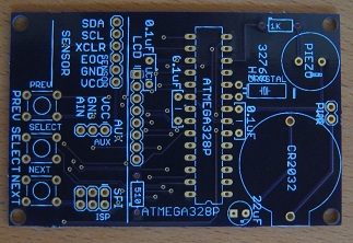
The total parts cost for either version of the Backcountry Logger is about $40. The Logger Classic can be assembled in an hour or two, and is fairly easy to build. The Logger Mini is more challenging to build, due to the use of surface-mount parts, but the result is a much more compact and professional-looking device. You can also build the Backcountry Logger on a breadboard, following the Logger Classic schematics.
PCBs can be made using the Gerbers included in the file distribution, but to kick things off, I’m giving away some free PCBs for the Logger Classic and Logger Mini to those who are seriously interested in experimenting with it. Send me email and let me know what you plan to do with it, and if I like your story I’ll send you a PCB.
For the curious, the README from the file distribution is included here:
Copyright (c) 2011 Stephen Chamberlin. All rights reserved.
Backcountry Logger by Stephen Chamberlin is licensed under a
Creative Commons Attribution-NonCommercial-ShareAlike 3.0 Unported License. (CC BY-NC-SA 3.0)
The terms of the license may be viewed at http://creativecommons.org/licenses/by-nc-sa/3.0/
Based on a work at www.bigmessowires.com.
Permissions beyond the scope of this license may be available at www.bigmessowires.com.
BUILDING YOUR BACKCOUNTRY LOGGER
1. Buy the required parts. The total cost should be about $40 USD. The parts required depend on which version of the logger you want to
build. See partlist.txt for the list of required parts.
2. Make or buy the circuit board (PCB), or prepare a breadboard. Visit www.bigmessowires.com and ask if I have any extra boards left. If
not, send the included Gerber files to a PCB prototyping service, and they can manufacture a board for about $25. If you are building the
logger on a breadboard instead of a PCB, follow the instructions for the Logger Classic.
3. Assemble the board. The Logger Classic uses all through-hole parts, and can be assembled in an hour or two. The Logger Mini uses all
surface-mount parts, and is more challenging to assemble, but can still be assembled by hand (I did it!).
Logger Classic:
The BMP085 breakout board comes without the header attached, so you must solder your own header to it. Solder male header to the *same*
side as the BMP085 chip. When you later mount the breakout board onto the socket on the main board, it should be upside down, with the
BMP085 on the underside, hidden from view.
Logger Mini:
The SQ-SEN-200 vibration sensor can be omitted. This part is only available directly from Signal Quest, with a minimum order quanity of
20. If omitted, the trip timer feature will not work.
The schematic and board layout show an external EEPROM chip. This was originally intended to store longer-term or higher-resolution
altitude/temperature data, but the firmware doesn’t use it. It can be omitted.
The bare BMP085 chip is difficult to hand-solder, because the pins are on its bottom, inaccessable with a soldering iron. To solder it,
first tin all 8 pads on the PCB with a small amount of solder. Make sure the heights of the solder blobs are as even as possible from pad
to pad. Next, apply flux to the BMP085 pins, and place it in position on top of the tinned pads. While pushing down on the chip from above
with a pick, heat the exposed portion of each PCB pad, one at a time, until the solder melts. The heat will be conducted along the pad,
under the chip, and the molten solder will bond to the hidden BMP085 pin. You may need to repeat this procedure several times to get a good
solder connection.
There may be a clearance problem between the battery holder and a few of the surface-mount components closest to it. If necessary, cut
away a small portion of the battery holder plastic with a knife to make it fit. Do not cut away any more plastic than necessary, or the
battery holder may bend when a battery is inserted.
4. Get an AVR programmer. I use the AVRISP mkII, which is $35 from Digi-Key. The $22 USBtinyISP AVR programmer is another popular choice:
see http://www.adafruit.com/products/46
5. Install the battery.
6. Connect the programmer to the board’s ISP header. Run AVR Studio, avrdude, or other AVR programming software. Confirm that the board is
working electrically, but connecting to the AVR and reading the device ID.
7. Program the AVR with the Backcountry Logger firmware. Use the programming software to load the .hex file into the AVR’s Flash memory.
You can use the precompiled hikea.hex file, or compile the included C source files and make your own .hex file.
8. Set the EESAVE fuse on to prevent your altitude/temperature data from being erased every time you reprogram the AVR.
MODIFYING THE LOGGER
You are encouraged to experiment with changes to the Backcountry Logger software and hardware. If you make a change that you want to share,
please send it to me and I’ll include it in a new version of this distribution. If there is enough interest, I will make a project at
Sourceforge or a similar site, so people can collaborate on further Backcountry Logger development.
Some ideas for further development:
- Add more detailed analysis tools to the software. Rate of ascent graphs, day by day statistics comparisons, user-defined graph
timescales, etc. - Add a way to download the stored sample data to your PC.
- Preload the elevation profile of your expected route onto the logger before starting a trip, then compare measured altitude samples with
the preloaded profile to determine where you are. - Modify the Logger Mini software to make use of the external EEPROM, to store a longer sample history, or high-resolution samples.
- Make a version of the Logger Classic that uses the higher-resolution OLED found on the Mini. These OLED’s can be purchased on a breakout
board on eBay or from Adafruit: http://www.adafruit.com/products/326
COMPILING THE SOFTWARE
The Backcountry Logger source code was built with AVR Studio 5, and the hikea.avrgccproj file will only work with AVR Studio 5. If you are
using a different version of AVR Studio, or a different compiler entirely, you will need to create your own project file or makefile with
the following settings:
Logger Classic
define these symbols: LOGGER_CLASSIC, NOKIA_LCD, F_CPU=1000000
include these libraries: libm.a
change these fuses: EESAVE on. Fuse settings are low: 0x62, high: 0xD1, extended: 0xFF
Logger Mini
define these symbols: LOGGER_MINI, SSD1306_LCD, F_CPU=8000000, SHAKE_SENSOR (optional)
include these libraries: libm.a
change these fuses: EESAVE on, CKDIV8 off. Fuse settings are low: 0xE2, high: 0xD1, extended: 0xFF
Logger on a breadboard:
follow the instructions for Logger Classic.
If you want to use the original software as-is without compiling, you can also use the precompiled hikea.hex files in the Classic or Mini
subdirectories.
USING THE SCHEMATIC AND BOARD LAYOUT
The Eagle .sch and .brd files can be found in the Classic and Mini subdirectories. In addition to the standard Eagle libraries, you will
also need the SparkFun library, Adafruit library, and Big Mess o Wires library. The Sparkfun and Adafruit libraries can be downloaded from
their respective web sites.
https://github.com/sparkfun/SparkFun-Eagle-Library
http://www.ladyada.net/library/pcb/eaglelibrary.html
The BMOW library is included here, as big-mess-o-wires.lbr.
PIEZO BUZZER NOTE: The Logger Classic uses a Murata PKM13EPYH4002 piezo buzzer, which has a 5mm pin spacing. I was foolish and added a new
5mm piezo footprint to the Sparkfun library. Your version of the Sparkfun library will not have this footprint, so you will get an error
when opening the schematic of layout file. If you wish to use this same buzzer, you can find the appropriate part in the big-mess-o-wires
library, named PIEZO.
Logger Mini on the John Muir Trail
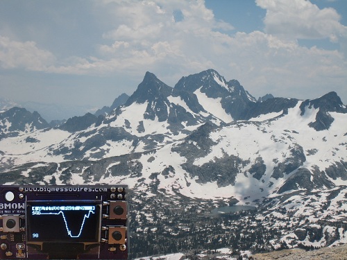
Logger Mini and I returned this week from the John Muir Trail. It was an amazing, epic trip, ending unexpectedly with me stranded in the middle of nowhere in the Owens Valley desert, gawking at the PLAGUE WARNING signs. It took me two days to get out, but I’m back home now and plague-free.
I used the logger quite a lot during the trip, and it worked like a champ. After a couple weeks of real-world use on the trail, a few points become clear:
- The trip timer feature (using a vibration sensor to detect movement) was totally pointless. It worked fairly well, but didn’t add anything of value, and I never used it even once. I’ll delete it and the associated hardware from future designs.
- Graphs going back more than 12 hours were also pointless. I never looked at them. That’s great, because it takes a lot of memory to store the sample data further in the past. I’ll delete the extra external EEPROM from future designs.
- Temperature measurement worked great for determining overnight lows, but not so great for highs or current daytime temperature. Inside its case, or in my pocket, or in the sun, it almost always showed a temperature that seemed unrealistically high. Maybe replace the minute-by-minute temperature graphs with daily high/low/avg stats instead.
- Where the logger really shone was the display of current and recent altitude. When we knew we were climbing towards a 12100 ft pass, and had been going for what seemed like hours, it was cool to pull out the logger and see exactly where we were and how much climbing was left.
- The screen was difficult to read in direct sunlight, where difficult means “impossible”. I knew this already, but it was still annoying.
- Reliability was excellent. I never experienced a single problem or unexplained reset on the trail.
- Battery life was excellent. My prototype is still on its original AAA battery, and the battery voltage has barely changed since I first installed it.
- There’s definitely a place for the logger, even in a GPS world. I also had a GPS along, but the logger is 20% of its size and 10% of its weight. The GPS chewed through batteries, had difficulty getting an accurate position fix, and exhibited poor alitutude accuracy even when it had a fix.
Overall, bringing along the logger was a clear success. So, what next? My inclination at this point is to share all the hardware and software design data, and try to get some additional people interested in improving the design further. I think there’s a place for both the Logger Mini and Logger Classic. The Classic is all through-hole parts and can be assembled in about an hour. The Mini is smaller and cooler, but more challenging to assemble. While the underlying hardware is different, the programming model is nearly identical, and the same software can be compiled for either device with only a few device-specific sections to reflect the different display screens. I have a few more unpopulated PCBs of both types that I can offer to developers, or put the Eagle and Gerber files somewhere and let people do what they like with them. Anyone have any other specific suggestions? It would be great to see this grow into something big.
Read 3 comments and join the conversation