

Backcountry Logger Bill of Materials
 The first Backcountry Logger prototype has gotten a very positive response from everyone I’ve showed it too, so I’m toying with the idea of making a few and selling them. I put together a bill of materials to estimate the cost, using the newest “shrunken” v3 prototype that’s designed but not yet built (still waiting for PCB and parts to arrive). As designed, the BOM cost is $32.01 each for quanity 100. That doesn’t include the PCB itself (probably a dollar or less for that quantity), the cost of assembly, or a case. For a quantity 1 prototype, the BOM cost is $37.20, but that assumes acquiring some parts as samples/free that aren’t for sale in individual quantities.
In addition to being smaller, the Logger v3 actually has more features than the v2 prototype shown in the photo here. The features require additional parts that increase the cost:
- $4.95: external EEPROM memory (allows storing more data samples and at higher resolution)
- $2.76: voltage booster/regulator (necessary because v3 uses a 1.5V AAA battery instead of 3V CR2032 watch battery)
- $4.58: vibration sensor (this is a totally new feature I added, to detect when you’re in motion and attempt to count your steps)
To build the v2 design, you could omit all those parts and lower the BOM cost to about $20.
The cost could likely be lowered further by searching for the cheapest component suppliers (I just used Digi-Key for everything), and by tweaking the design to use fewer and cheaper components.
| Quantity | Part | Purpose | Supplier | Price @ 1 | Ext Price @ 1 | Price @ 100 | Ext Price @ 100 |
| 1 | ATmega328P-AU | microcontroller | Digi-Key | $4.87 | $4.87 | $3.06 | $3.06 |
| 1 | MAX1675EUA+ | voltage regulator | Digi-Key | $5.73 | $5.73 | $2.76 | $2.76 |
| 1 | M24M01-RMN6TP | EEPROM | Digi-Key | $6.75 | $6.75 | $4.95 | $4.95 |
| 1 | BMP085 | pressure sensor | Digi-Key | $3.81 | $3.81 | $3.81 | $3.81 |
| 1 | UG-2864HSWEG01 | 128×64 OLED display | wide.hk | $7.99 | $7.99 | $4.70 | $4.70 |
| 1 | CCV-084B16 | buzzer | Digi-Key | $2.36 | $2.36 | $1.96 | $1.96 |
| 1 | SQ-SEN-200 | vibration sensor | SignalQuest | N/A | $0.00 | $4.58 | $4.58 |
| 1 | CFS206-32.768KDZF | crystal oscillator | Digi-Key | $0.28 | $0.28 | $0.16 | $0.16 |
| 1 | UP1B-220-R | inductor | Digi-Key | $1.38 | $1.38 | $1.06 | $1.06 |
| 1 | MBR0520L | Schottky diode | Digi-Key | $0.63 | $0.63 | $0.20 | $0.20 |
| 3 | B3FS-1010 | tactile switch | Digi-Key | $0.65 | $1.95 | $0.47 | $1.41 |
| 1 | 2466K-ND | AAA battery holder | Digi-Key | $1.45 | $1.45 | $1.21 | $1.21 |
| 10 | 0805 0.1uF ceramic | capacitor | Digi-Key | N/A | $0.00 | $0.03 | $0.30 |
| 4 | 0805 1.0uF ceramic | capacitor | Digi-Key | N/A | $0.00 | $0.06 | $0.24 |
| 2 | 0805 2.2uF ceramic | capacitor | Digi-Key | N/A | $0.00 | $0.08 | $0.16 |
| 2 | 0805 47uF tantalum | capacitor | Digi-Key | N/A | $0.00 | $0.71 | $1.42 |
| 2 | 0805 4.7K ohm | resistor | Digi-Key | N/A | $0.00 | $0.01 | $0.02 |
| 1 | 0805 390 ohm | resistor | Digi-Key | N/A | $0.00 | $0.01 | $0.01 |
| $37.20 | $32.01 |
JTAG, EXTEST, and hair loss
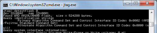 Oof. See that window to the left? That’s the result of 10 hours of debugging effort on bring-up for my custom Tiny CPU board. What you see is UrJTAG connected to the JTAG interface of the Max II CPLD, and successfully detecting the 29LV040B flash ROM that’s also on the board. Getting to this point was a long process covering everything from software to cleaning up bad solder joints.
The good news: I’ve soldered the Max II CPLD, Flash ROM, and SRAM to the board, and they seem to be working. By using UrJTAG and the EXTEST instruction, it’s possible to disconnect the CPLD’s core logic from the pins, and set the pin states to any arbitrary values. The software also needs to be told which pins are connected to the address bus, data bus, CS, OE, and WE. Once that’s done, it’s possible to read and write any non-JTAG device whose pins are connected to the CPLD, by bit-twiddling the CPLD pins. Using UrJTAG’s commands for memory access, I’ve successfully written and read from the on-board SRAM, and reprogrammed the on-board Flash ROM. That should be nearly everything that’s needed to start work on the Tiny CPU core itself.
Interaction with the Programmed Design
I find JTAG and especially the UrJTAG tool to be maddeningly difficult to understand. Things don’t work how I’d expect, or don’t work at all, and I can’t be certain if it’s a hardware problem, software bug, or misunderstanding on my part. The best example is the reason that it took me so long to reach the point where the Flash ROM was successfully detected: interaction between the core logic (the design programmed into the CPLD) and the EXTEST pin manipulation. From what I’ve read, there should be no interaction. When the EXTEST instruction is executed by the JTAG controller, then the pins should be decoupled from the core logic. It shouldn’t matter at all what design is programmed into the CPLD, what that design wants to do with the pins, or whether any design is programmed at all.
After long experimentation and electrical testing, I discovered that the core logic design does matter when interfacing to other devices with EXTEST. Whether this is normal, or the result of a boundary scan software bug in UrJTAG, I don’t know. What I found is that if I programmed the CPLD with a design that declared the data bus as type inout (which it is, of course), then I could read from the SRAM and Flash but not write to them. By sticking a multimeter on the pins, I found that data bus pins driven to a logical 0 using EXTEST worked fine, but data bus pins driven to a logical 1 just went into a high-Z state instead, so I could never write a ‘1’ bit. I also learned that if I set the data bus type as output, then I could no longer read from the RAM or Flash. Only when I set the data bus type to input could I both read and write using EXTEST. This is nonsense on a several levels, as it shouldn’t be necessary to reprogram the CPLD with a new design just to use the EXTEST functionality. The only explanation I can think of is that the boundary scan register uses 3 bits to define the state of each pin (input, input with pull-up, output driving 0, output driving 1, output driving Z, and a few others) which UrJTAG may not handle properly, with some bits carrying over from the programmed design. I had a similar problem when using a trial version of TopJTAG Flash Programmer, however, so I’m not sure I can blame the software.
JTAG Bit-Banging
As another example of UrJTAG strangeness, the board has an LED connected to IO97, such that the LED illuminates when the pin value is 0. It should be possible to blink the LED using UrJTAG’s set signal command, e.g:
jtag> set signal IO97 out 0
After much tearing out of my hair, I learned that while that’s part of it, it’s also necessary to explicitly put the device in EXTEST instruction mode first, and explicitly shift the instruction and data into the device, as UrJTAG does none of this for you:
jtag> instruction EXTEST
jtag> shift ir
jtag> set signal IO97 out 0
jtag> shift dr   (the LED turns on)
A little cumbersome, but at least it works. In contrast, I was never able to get the corresponding get signal command to work at all. After setting IO97 to 0 as above, which visibly turns on the LED, the value of IO97 still reads as 1:
jtag> get signal IO97
IO97 = 1
jtag> shift dr
jtag> get signal IO97
IO97 = 1
The ability to twiddle pins arbitrarily through JTAG could be a huge aid to debugging, but not if the corresponding ability to read the current pin state doesn’t work.
If anyone has some experience using UrJTAG for this kind of troubleshooting, please leave a comment, or contact me by email. Thanks!
Read 5 comments and join the conversationSoldering, with Profanity
Hot diggety damn! I believe I’ve successfully soldered the Max II in its cruel 100-pin package with 0.5 mm pin spacing. At least, I’ve assembled enough of the board to connect it to a JTAG programmer, program an LED blinky routine to the Max II, and confirm that it works. There could still be all kinds of pins shorted or broken, of course, but at least I know I didn’t fry it completely.
Soldering that chip wasn’t fun. It took me about two hours just for that single TQFP 100. I used the drag soldering technique, where you goob tons of solder onto the pins and create pin-to-pin solder jumpers like crazy, then go back afterwards with solder wick to clean up the jumpers. At least that’s the idea.
I had the absolute worst time trying to wick away the jumpers. No matter what I did, the extra solder on the pins wouldn’t soak into the solder wick. I set the wick on top of the pins that had jumpers, then set my iron on the wick, and pressed down onto the sandwich. The solder underneath the wick would melt, but it wouldn’t go anywhere. When I removed the iron and wick, the jumpers remained right where they’d been, with nothing at all soaked into the wick. I applied flux everywhere, over and over, but it didn’t help.
This pattern went on for ages, and I got more and more upset. I started swearing at the board, using every profanity I could think of. I had to close the windows so the neighbors wouldn’t hear. After a while, I started singing random profanities to the tune of opera while I worked on the jumpers. I burned the soldermask off several of the traces, burned the board, and re-heated the same pins so many times that I was certain nothing was left inside the chip but melted slag. All in all, it was not a good time.
Eventually I stumbled onto a few techniques that helped a little, raising my wicking success rate from 0.1% to maybe 20%.
- Some jumpers can be cleared simply by touching the iron briefly to the pins, without any wick.
- Don’t stretch out the wick braid. Keep the strands pressed together, like stranded wire.
- If a stubborn bit of solder refuses to be wicked away, add more solder. A huge glob is actually easier to remove than a tiny fleck.
Assuming the other as-yet-untested pins on the Max II are OK, then assembling the rest of the board should be cake.
Read 4 comments and join the conversationTiny CPU Boards
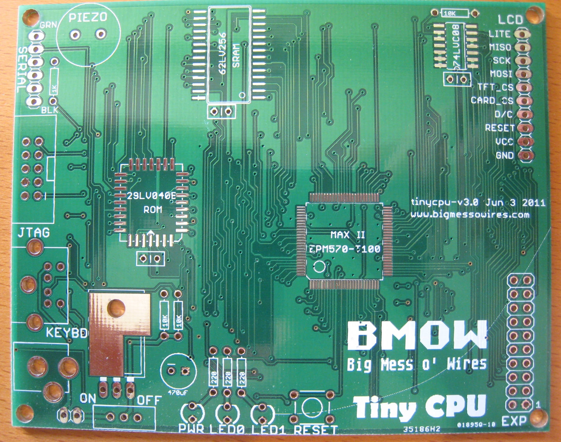 The Tiny CPU boards arrived yesterday from Seeed Studio’s Fusion PCB service. Now it’s time to break out my soldering iron again, and get busy with that 0.5 mm pitch 100-pin TQFP. Ugh!
I placed the order with Seeed on June 6, and received the boards on June 23, so that’s 17 days of calendar time from order to mailbox. Considering how slow shipping from China can be, I’m pretty happy with that. It’s actually not much slower than the 12 day turn-around time I got from Dorkbot PDX’s PCB service, which is done in the USA.
The Tiny CPU board is 100mm x 80mm, or about 12.4 square inches. For 10 boards with 50% e-test, the cost was $25 plus about $7 for shipping. I actually received 12 boards instead of the promised 10. Five boards were taped together and marked with a black line down the edge, so I assume those are the ones that were e-tested. The other seven boards were stacked on top, then the whole bundle of 12 boards was shrink-wrapped, packed in bubble wrap, and packed in a small box for shipping.
The quality of the boards looks pretty good, especially considering the dirt cheap price. Drill holes look nicely centered, and tracks look neat and clean. It’s not all perfect though, and the overall quality level feels a bit less than the Dorkbot PDX boards. There’s a bit of variation in soldermask and plating from board to board, and some of the boards look pretty scuffed up. There are also some odd numbers and a line that were added to my silkscreen layer, which I could do without.
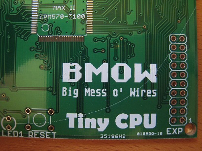 Um, what the heck is 35186H2 and 01895Q-10? And moreover, what is that curved arc in the silkscreen layer extending from LED1 all the way to the board’s edge? None of that appears in my top silkscreen Gerber. It’s not a huge deal to have some random extra numbers and lines, it doesn’t affect anything of course, but it’s a bit annoying.
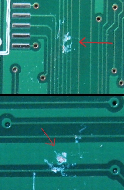 Two of the boards have some pretty significant damage from scraping or impact. I’m not sure if it’s enough to cause a failure, but it definitely might. One board is damaged on the top, and the other on the bottom, and when you stack them the damaged spots overlap. I’m guessing some sharp object got caught between these two boards, and ground away the soldermask where it rubbed against them. Maybe this is why I got 12 boards instead of 10?
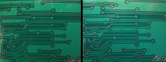 I tented my vias with soldermask this time, or tried to anyway. In theory, 100% of the vias should be tented. In practice, most of the vias are tented, but some aren’t, and the fraction of tented vias varies quite a bit from board to board. Here’s the same section from two different boards, where one is 100% tented and the other is maybe 25%.
Overall I’m fairly happy with these Seeed PCB Fusion boards: decent build quality and cheap pricing. Yes, there are a few dinged and damaged boards, but given the total number of boards for the price (and the two bonus boards I received), I can call those throw-aways and still have a good deal. I would certainly use them again. For smaller boards where the costs are comparable, though, I would favor Dorkbot PDX’s PCB service, since it’s a few days faster and seems to be a bit higher quality.
Backcountry Logger v1 Demo
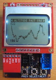
The Backcountry Logger is a portable microcontroller-driven device that collects temperature, air pressure, and altitude data, and shows graphs on a built-in screen. It’s intended for hikers, climbers, skiers, and other outdoorsy folks who want to geek out with environmenal data about their activities.
I’ve written extensively already about the design and board layout of the Backcountry Logger, but never described its actual usage in any detail until now. I’d been waiting until I received the custom-designed board back from the PCB house, so I could move the project off the protoboard and onto a permanent frame. The board finally arrived a few days ago, and I had everything assembled after about an hour of soldering. It all worked flawlessly right away, so the transition from protoboard to PCB was very smooth.
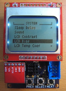
 The logger interface is organized as 16 different screens, and the user cycles through the list of screens using the PREV and NEXT buttons. Each screen displays status text or a graph of historical data. Most screens also have a menu that can be opened with the SELECT button, providing access to further customization and configuration options. Screens are grouped into altitude, temperature, and air pressure sections, with each section having historical graphs at time scales ranging between past 90 minutes to past 14 days.
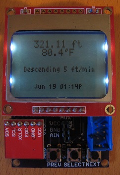
The main screen shows a customizable summary of environmental data. By default it displays current altitude and temperature, rate of ascent, and time of day, but the contents are fully customizable from the menu. Each of the screen’s six lines can be configured to show one of eleven different statistics, such as weather forecast, current air pressure, and estimated time to a previously-set goal altitude.
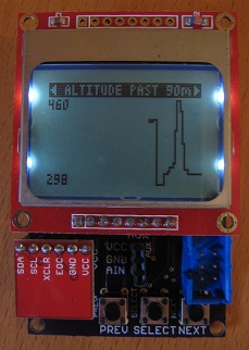 One of my first tests was to take the logger up a nearby hill. Here you can see the 90-minute altitude graph from the test. The graph only goes back about 30 minutes, to the time when I inserted the battery and data collection began. The graph begins with a big spike down to about 300 feet when I calibrated the altitude. I then got in my car, and drove up a hill that’s about 470 feet according to the topo map. At this scale, each pixel on the X-axis reperesents one minute.
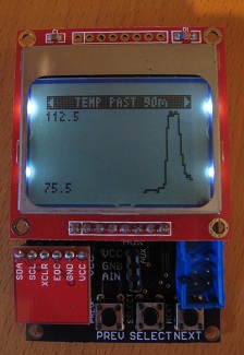 Here’s the 90-minute temperature graph from the same test. It was a hot day, and my car had been sitting out in the sun, so the interior of the car was sweltering. How sweltering? About 112F, according to the logger. Yikes!
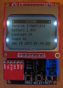
 The system screen contains lots of goodies like the firmware version number, current battery voltage, and LCD contrast setting. The system settings can all be edited via the screen’s menu.
 This version of the Backcountry Logger is about 7 cm long, 4.5 cm wide, 2 cm tall, and weighs 1.3 ounces. It uses a 3V CR2032 battery, unregulated. The current consumption is about 1.5 mA when it’s on, and 20 uA when it’s asleep. Depending on how much it’s used, the battery life should be about 8-12 months.
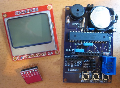
The main board has only one IC: an ATmega328P. The rest of the space is consumed by the battery, piezo speaker, buttons, a few passive components, and headers. The LCD and BMP085 pressure/temperature sensor are mounted on breakout boards that plug into the headers.
I’m planning to make a version 3 of the Backcountry Logger that’s substantially smaller and lighter. (Don’t ask what happened to version 2.) This version will be just 5 x 3 cm, and will use a tiny OLED screen that’s higher-resolution than the LCD but physically much smaller. All the parts in version 3 will be surface mount, instead of this version’s through-hole parts. Because the OLED requires more current than the LCD, version 3 will use a single AAA battery with a voltage booster in place of the CR2032 battery. Check back in a few weeks, and I hope to have a version 3 demo to share.
Backcountry Logger v1 PCB
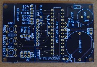 Hooray, the v1 Backcountry Logger boards have arrived from the PCB manufacturer! This time I used Dorkbot PDX, and the elapsed time from the ordering cutoff date to board delivery was only 12 calendar days. For $5 per square inch, with three copies of your board, and free shipping in the USA, I call that a pretty good deal.
 The boards have dark purple soldermask, with gold plating. The quality looks good. When I received them, the boards originally had several small tabs around the edges from the panelization process. These were easily broken off with a pair of pliers, but you can still see some slight rough spots on the edges where the tabs were.
Before I even begin to stuff the board with components, let’s count all the mistakes I already see. You can’t learn without making mistakes, and I sure made a few here.
- silkscreen layers– I delivered an Eagle .brd file for manufacturing, and I thought the silkscreen would include only the contents of Eagle’s tPlace layer. Instead, both the tPlace and tNames layers appear on the silkscreen, which results in a lot of unintended and overlapping silkscreen labels. Next time I’ll deliver individual Gerber files instead of the .brd file, so I can be sure what it will look like.
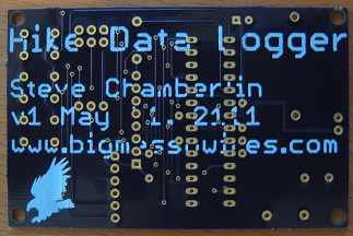
- silkscreen on pads – You can’t just run silkscreen text right across the pads… what was I thinking? Wherever text overlaps a pad, the text disappears. This makes the text on the bottom side with my name and date very difficult to read..
- text proofreading – The date text says “May 21, 2111”. It’s from the future!
- no ground plane – I forgot to include a ground plane. Fortunately with this simple, low-speed design it’s probably OK without one, but its omission was not intentional.
- untented vias – I meant to tent the vias (cover them with soldermask), but I forgot. With tented vias, they wouldn’t stand out so much, and text running on top of vias would be much more legible.
- narrow pad holes – Some of the pads have what appear to be very narrow holes. It’s tough to see in the photo, but the holes for the ATmega and the capacitors are substantially narrower than all the others. Of course the hole sizes comes from the part footprints, which I just took from the Eagle library, but it’s my fault for not checking them. I did a quick test fit, and I think everything will still be OK with the narrow holes, but it’s tight.
- insufficient part clearance – I kind of assumed that parts would exactly match their outlines in the library, but a few are bigger. The battery holder in particular is a bit bigger than its outline, enough so that it partly blocks the power jumper (right-center), and bypass capacitor next to the ATmega.
- mounting holes too big – The four mounting holes in the corners are bigger and closer to the edges than I intended. The footprint for the hole is two concentric circles, and I’d thought the inner circle was the hole itself and the outer circle was the screw head for the matching screw. Instead, the outer circle is the hole itself, and I don’t know what the inner circle is.
- soldermask on pads – The two resistors both have soldermask covering their top-side pads. If you look closely, you can see that the 1K resistor at top-right, and 510 Ohm resistor at the bottom-middle don’t have visible pads. They’re there, but covered. Fortunately the bottom side of the pads aren’t covered, and that’s the solder side, so it’s OK. I checked Eagle, and this is how the Sparkfun axial PTH resistor footprint is designed, so it’s intentional. I can’t imagine why though– it seems like a bad idea.
Now it’s time to put this thing together. Soldering iron, here we go!
Read 6 comments and join the conversation