

Shrinking the Backcountry Logger
 Shrinking a design as far as possible can be an addictive hobby. Even though PCBs for the first backcountry logger design aren’t yet back from the board house, I’ve been busy working on a revised version that’s just 1.9 x 1.1 inches (49 x 28 mm). That’s about the size of 3 AAA batteries laid side-by-side. It’s small!
If you’re just tuning in, the backcountry logger concept is a portable ATmega-powered device that collects temperature, air pressure, and altitude data, and shows graphs on a built-in LCD screen. It’s intended for hikers, climbers, and other outdoorsy folks who want to know if it was colder last night than three nights ago, whether the ridge they’re on is the 10200′ or 10600′ one from the map, or whether a storm is likely soon. Much attention has been giving to minimizing power consumption, so the battery should last many months.
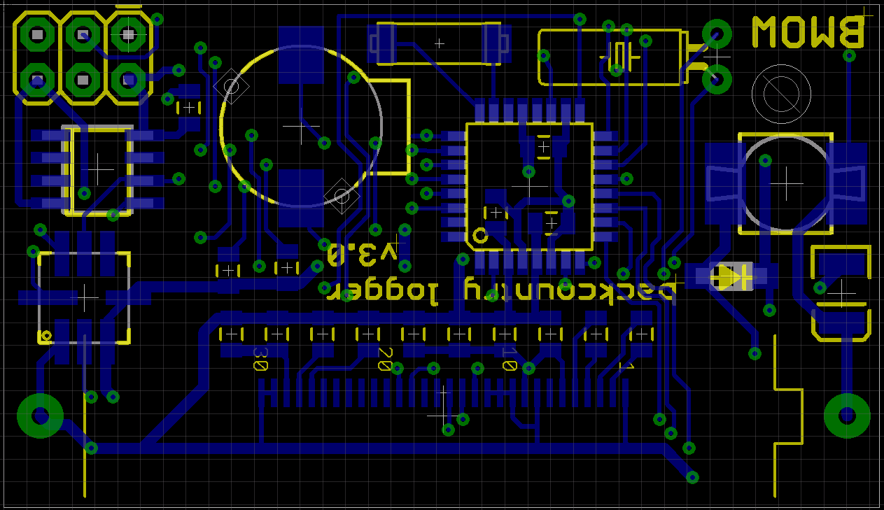
 Here’s the original logger design. It’s 2.75 x 1.8 inches, and uses all through-hole parts. The LCD is a Nokia 5110 on a breakout board, mounted onto the main board with an 8-pin 0.1 inch header, and covering the upper two-thirds of the main board. Similarly, the Bosch BMP085 temperature and pressure sensor is on a second breakout, mounted with a 6-pin 0.1 inch header and covering the lower-left corner of the main board. The battery is a CR2032 coin cell, and projected battery life is 8-12 months.
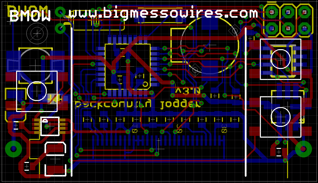
While the new design is functionally similar to the original, it replaces virtually every component with a smaller SMD version. It also drops the breakout boards, soldering the components directly to the main board instead. The LCD is replaced by a 128 x 64 OLED, which is physically smaller but has a higher resolution. To meet the higher power demands of the OLED, the coin cell is replaced by a single AAA cell and a 3.3V boost regulator. The addition of an external EEPROM provides space for higher resolution or longer-term data storage than is possible with the ATmega’s built-in EEPROM. And as a last-minute addition, the new design also adds a SignalQuest SQ-SEN-200 omnidirectional tilt and vibration sensor, which I hope to use to measure periods of movement to compile trip duration stats. Projected battery life is about 5 months.
 The majority of the top layer is covered by the OLED itself, leaving precious little space for component placement. It’s just the three tactile switches, boost regulator IC, and a couple of capacitors. The tactile switches are the thinnest I could find (2.6 mm), so as not to add too much to the overall thickness of the logger. I would have dearly loved to use the user-friendly switches with the 12mm base, but there simply wasn’t enough room. Instead, the switches here are the 6mm base type with a 3mm round button. A single drill hole in the top-left corner provides an option to wear the logger on a lanyard or keychain.
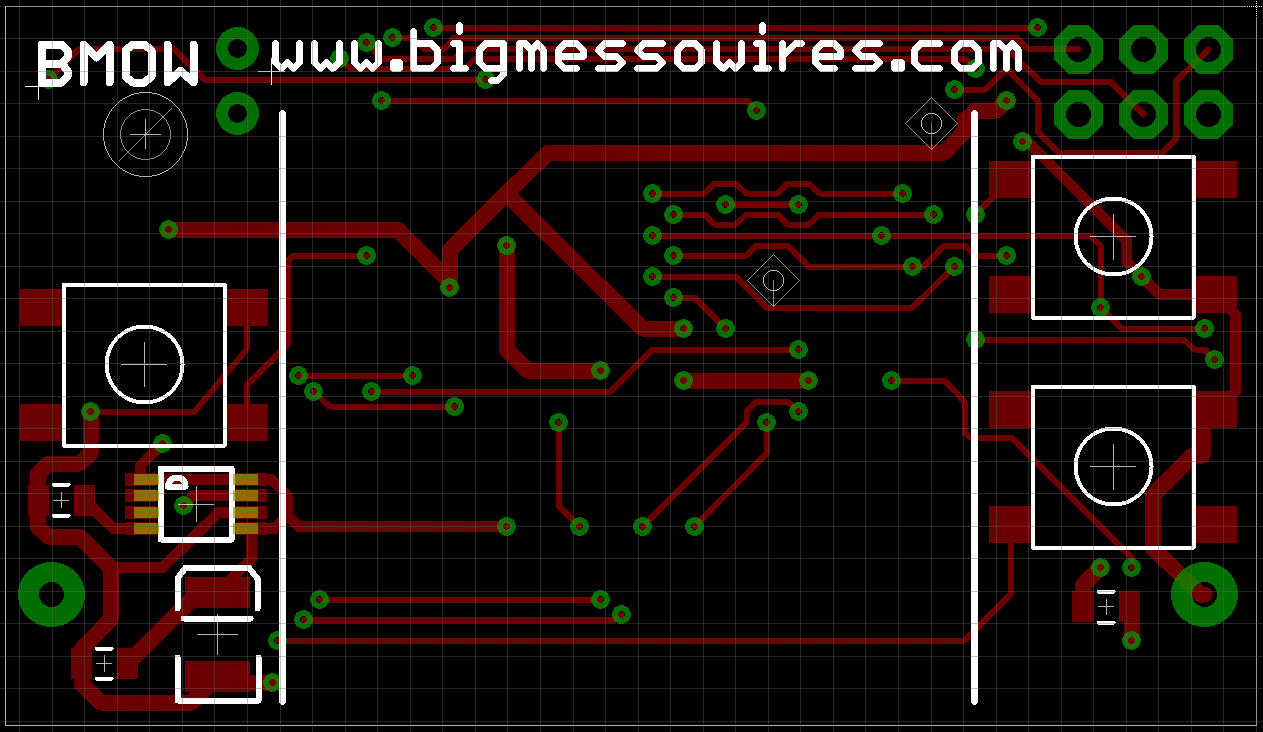
 The bottom layer is were most of the action is. The ribbon connector from the OLED wraps around the bottom of the board, and its 30 pins are soldered at bottom-center. The AAA battery spans the bottom third of the board, lying on top of the ribbon connector. Down the left side are the ISP header, external EEPROM, and BMP085 sensor. The right side is occupied by an inductor, diode, and capacitor required by the boost regulator. Squeezed into the center is the ATmega 328 in TQFP package, a tiny speaker, 32 kHz crystal, and the SQ-SEN-200 vibration sensor. The SQ-SEN-200 is the barrel-shaped component at top center, and its internal switch chatters open and closed whenever it’s bumped or moved.
Cramming all these components into the space available was an interesting challenge. The resulting board is almost as small as theoretically possible, since the width is already constrained by the size of the battery, and the height could only be a few mm less before it would be shorter than the OLED screen. I plan to wait a while before sending this board for manufacturing, at least until I’ve received the boards for the original design and confirmed that everything works. All this waiting for boards is maddening!
Read 7 comments and join the conversationLow-Power LCD Smackdown
 Sometimes it seems like there are a million different LCDs you might use with your microcontroller project, and deciding on one can be hard. Once you’re ready to move beyond a basic text display, you’ll find graphic displays have a dizzying number of options for technology, color depth, interface type, driver, and power. Recently I’ve been collecting info on display options for my own projects, and here I’m presenting three options that look promising.
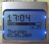
The Nokia 5110 is a low-resolution monochrome LCD that’s cheap and extremely low-power. A family of small monochrome OLEDs provide crisp, bright displays with a bit more resolution, in a teeny-tiny package. A 1.8 inch color TFT provides even greater resolution and 18-bit color, while still limiting power to about 90 milliwatts.
 Nokia 5110
Colors: monochrome
Resolution: 84 x 48
Active display area: 2.8 x 2 cm
Interface: SPI
Power: 3.3v
Current: 0.4 mA for logic, 1-10 mA for backlight
Cost: $10
Vendors: Sparkfun, Adafruit
This is the display I’m currently using for my Backcountry Logger project. It’s cheap, easy to use, and consumes very little power. You don’t really need the backlight for daytime visibility, and with backlight off, it consumes just 400 uA! Awesome for battery-powered projects. Just 1-2 mA worth of backlight current is plenty for night-time visibility too, although more would be nicer. This puts the display well within the capabilities of a single CR2032 coin cell.
Working with the display is simple, as long as you remeber it’s a 3.3v device and not 5v tolerant. There are lots of great tutorials and examples available for this display, including this nice one from Adafruit. Communication with the display controller uses SPI. Writing a single byte sets 8 pixels at a time, so pixels are not individually addressable. If you’re mostly displaying text or bitmaps this isn’t a problem, but if you need a more complex image consisting of many overlapping elements, you’ll need to composite them in software before sending the result to the display.
The weak points of the Nokia 5110 display are resolution and looks. The contrast and sharpness are pretty good for a display of this type, but there’s still no getting around the fact that this is a low-res, dark-gray on light-gray display. The 84 x 48 resolution allows for just 14 x 6 characters using a typical 5 x 7 font (allowing for space between letters). If you seek utility, low cost, and low power, it’s a great solution. If you want something with a bit more bling, look elsewhere.
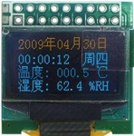 SSD1306/SSD1308 OLED
Colors: monochrome
Resolution: 128 x 64
Active display area: 2.4 x 1.2 cm
Interface: SPI, I2C, or parallel
Power: 3.3v, and maybe 7-12v
Current: roughly 5-13 mA, depending on how many pixels are lit
Cost: $15-$20
Vendors: Sparkfun (bare LCD), Adafruit, eBay
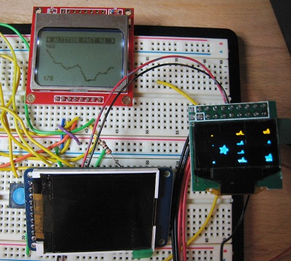
This little OLED display comes in a few slightly different flavors, but all of them are tiny. It’s one thing to read the dimensions (0.96 inches horizontally), but another to see it in person. All three of the displays discussed here are small, but this particular OLED is smaller than a postage stamp. It’s about the size of the last joint on my thumb.
Despite its small size, the OLED display is very readable. It’s sharp and bright, and a pleasure to look at. Since it’s an OLED, there’s no backlight, and current draw varies between about 5 to 13 mA in my testing, depending on how many pixels are illuminated. The 128 x 64 resolution is a nice bump from the Nokia 5110 display, allowing for 21 x 8 characters. Communication choices are SPI, I2C, or parallel, selectable via configuration pins. Like the Nokia, each byte sets 8 pixels at a time. Adafruit has a tutorial and library.
The display controller chip runs at 3.3v, and the display itself needs 7-12v, although you might be able to get away with a single supply depending on which display variant you have.
Adafruit sells this display on a break-out board, with white pixels, with a SSD1306 controller. The SSD1306 has a built-in charge pump, and can optionally generate 7.5v for the display from a 3.3v supply, which is a very convenient option. Sparkfun sells the naked LCD, with white or blue pixels, and a SSD1308 controller that lacks the charge pump. You’ll need to mount the 0.5 mm pitch connector somehow, and provide a separate power supply for the logic and display. The most common eBay variant comes on a break-out board, with the SSD1306 controller, and yellow pixels in the top quarter and blue pixels in the bottom three quarters. Mine also came hard-wired to use the parallel interface, and switching to SPI required wicking away some solder jumpers and adding new ones.
This display meets a narrower range of needs, but is awesome for its target niche. I’m strongly considering doing a version 2.0 of the Backcountry Logger using this display, to gain the benefit of smaller size, higher resolution, and better looks. Unfortunately with the amount of current it needs, it’s probably outside of what a CR2032 can provide, and will require 2 x AAA or 1 x AAA with a DC boost converter.
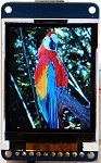 Adafruit 1.8 inch TFT
Colors: 18-bit (262144 colors)
Resolution: 160 x 120
Active display area: 3.6 x 2.8 cm
Interface: SPI
Power: 5v or 3.3v
Current: 1 mA for logic, about 26 mA for backlight (can be dimmed)
Cost: $25
Vendors: Adafruit
This is the display I plan to use for Tiny CPU. Unlike the others, it’s a full color display with individually addressable pixels. It supports 18-bit color, but can also be configured for 16-bit color or monochrome (I think? Haven’t tried that yet). It’s a bit larger than the other two, but still quite small compared to most displays. It is natively a 3.3v device, but the Adafruit breakout board includes an LDO regulator and level-shifter chip, so it can be used with 5v microcontrollers as well. Current demands are the highest of the three displays, but not excessive at about 1 mA for logic and 26 mA for the backlight. The backlight can be dimmed using PWM to further reduce the current. This is still well within the capabilities of an AAA-based battery-powered project.
The TFT is very attractive, not quite on par with the OLED, but certainly nicer than the CSTN used in some other cheap color LCDs. The 160 x 120 resolution feels giant in comparison with the previous displays, allowing for 26 x 15 characters. The display controller allows for a few different protocols, but the break-out board hard-wires it for SPI.
With the larger resolution and greater bit depth, a screen’s worth of data requires many more bytes than the previous two displays. Depending on the speed of your microcontroller and SPI interface, this may result in noticeably slower refresh times. I tested it using hardware SPI on a 16 MHz Arduino, and found the refresh time to be acceptable.
Adafruit has a nice tutorial and library for working with this display (I’m sensing a theme here). Unexpectedly, the breakout board also has a micro-SD card reader on it. Ignore it, or use it as a bonus peripheral in your next project.
Read 6 comments and join the conversationOff To The Board House
 The Tiny CPU board design is now off to the board house for manufacturing. The three week wait begins. Somewhere during that time, the Backcountry Logger boards should come back too.
I selected Seeed Studio’s Fusion PCB service, because it was by far the cheapest prototype-oriented board house for a board this size (12.4 sqin) with multiple copies. I’m a little worried, though, because the Fusion PCB CAM file for Eagle appears to have a bug. I don’t know much about what the CAM file does, other than that Eagle uses it to generate the individual Gerber files from the Eagle .brd file, and all the board houses I’m aware of provide a CAM file you’re supposed to use. Using the Fusion PCB CAM file, and viewing the resulting Gerbers in gerbv, all the drill holes were offset about 250 mils below-left relative to the other layers. You can see this in the image above: the drill holes are shown in pink, and are clearly misaligned with the top and bottom copper layers in blue and green.
Processing the same .brd with the CAM files for BatchPCB and Dorkbot PDX did not have this problem. In the end, I used the BatchPCB CAM file, and sent the resulting Gerbers to Seeed along with a note explaining what happened. Hopefully it will be fine.
After I sent the board for manufacturing, I had a nasty surprise when I went to order the parts. The particular SRAM and ROM types and packages were selected because they were cheap “closeout” deals at Jameco, my friendly neighborhood electronics supplier. I guess they weren’t kidding about them being closeouts, though, because when I returned to the Jameco web site to make a purchase, a few days after having selected those chips, they were no longer listed for sale. Doh!
I was able to find the same SRAM (an ISSI 62LV256 in SO14 package) at Digikey, but the Flash ROM (AM29LV040B in PLCC package) wasn’t available there or anywhere. Fortunately eBay saved the day, and I was able to get two for a few dollars. Lesson learned: buy the parts before you manufacture the board. Or choose more commonly-available parts instead of legacy parts on closeout.
Read 1 comment and join the conversationTiny CPU Board Design
 Whew! It was a big job, but I finished the Eagle board layout for the new Tiny CPU, using the Max II CPLD. The board is about 4×3 inches, and if your monitor has a typical 72 DPI, then the image to the left is actual size. It’s clear that soldering the 100 pins on the Max II is going to be a challenge. Click the image to see a higher-resolution version of my horrible component placement and routing.
Routing all those connections was a long, difficult job. You can see I left myself lots of extra space around the CPLD to help with routing, but the space between the CPLD, RAM, and ROM is still packed to the roof with traces.
I’m happy I was able to get all the traces to fit, since part-way through the task, success looked doubtful. Unfortunately I was forced to abandon the goal of routing all unused I/O pins to an expansion header, because I simply ran out of room. I managed to route 18 I/Os to the header, but the remainder of the unused I/Os are unconnected and unusable.
I’ll probably sit on this for a day or two, giving myself a chance to remember any last-minute stuff I forgot, before sending it to a board house for manufacturing. I’ll probably go with Seeed Studio this time, since ten copies of this 8x10cm board with 50% E-Test are only $25. Having ten copies will be a big help, when I melt the first few trying to solder those nano-scale pins!
Read 11 comments and join the conversationTiny CPU Rebirth?
With the Backcountry Data Logger more or less finished (just waiting for the PCB), my thoughts have returned to my neglected Tiny CPU project. I did a huge amount of design work on Tiny CPU about a year ago, finishing the complete CPU design in Verilog, as well as a companion design called Tiny Device for bank switching and peripheral I/O. I even built a test board using the target CPLD (a 128-macrocell Altera EPM7128), so I could experiment with JTAG programming and various construction issues. But then progress stalled, and there’s been nothing further for a year.
I lost interest in Tiny CPU. Why? I don’t fully understand it myself, but two reasons in particular are big contributors:
Questionable Value – There are lots of small soft CPU cores out there, with probably 100 different designs on opencores.org alone. Some of the better ones like PicoBlaze provide a very capable CPU that still fits a pretty small device. Or on the other end of the scale, soft CPUs like MCPU are academic masterpieces, fitting into the smallest devices, even if they aren’t very capable or practical as CPUs. Tiny CPU occupies an awkward middle ground where it requires nearly as large a device as PicoBlaze, yet provides not much more capability than MCPU. So what’s the point?
Construction Fatigue – After completing the Verilog design work, all that remained was to actually build a computer using Tiny CPU. I say “all” with some sarcasm, because designing the required PCB and working out all the necessary connections between the twin CPLDs and SRAM and ROM is a huge job, not to mention writing all the software needed to make it work. At the time, I was really much more interested in the CPU design work than the construction aspect of the project.
Not too much has changed since then, except that I’m more interested in custom PCB design and construction than I was before. I also hate to see a project abandoned half-finished, so I’m considering returning to Tiny CPU with a different focus. I can’t do much about the questionable value of Tiny CPU, but honestly, who ever said any of my projects had value? I can do something about the construction question, though, so that’s where I’ll focus my attention.
Enter the Max II
The original Tiny CPU design called for an Altera EPM7128, a comparatively old 5V device in a PLCC package, allowing for through-hole soldering with a PLCC socket. Tiny CPU and Tiny Device each required a separate CPLD, so there would be two of them on the computer board. I insisted on the EPM7128 because I wasn’t confident I could solder the surface mount packages that most newer devices use, and also because I liked the challenge of fitting 128 macrocells.
I’m now looking at using an Altera Max II, which is a much more modern CPLD with the equivalent of roughly 192 or 440 macrocells in the two smallest sizes. The Max II is a 3.3V device, so this change would involve moving all the other components in the system to 3.3V as well. Fortunately 3.3V SRAM, Flash ROM, and LCDs are pretty easy to find, so that’s not an issue. The only challenge would be the PS/2 keyboard interface. The keyboard data and clock signals are unidirectional in the Tiny CPU design, and use an open collector and pull-up resistor instead of actively driving 5V, so that wouldn’t be a problem. However, the keyboard itself would require a 5V supply.
Switching to the Max II would entail combining Tiny CPU and Tiny Device into a single CPLD, creating something that’s a bit more like a microcontroller than a traditional CPU. The Max II comes in a 100-pin TQFP package with 0.5mm pin spacing, so it would be a real challenge to solder, but I’ve been told repeatedly that it can be done.
The Max II also has a few other advantages. It has a built-in clock generator and power-on reset circuitry, allowing me to delete two external parts from my original design. It also has 1KB of internal Flash memory, which might be useful for bootstrapping.
The final advantage of the Max II, especially the 440 macrocell-equivalent version, is that it would provide some breathing room to recover from mistakes. The original Tiny CPU and Tiny Device designs both just barely fit the EPM7128, and any bugs discovered after construction might require fixes that would push them over the capacity of the device. Some combination of the tight fit and age of the device also gave Altera’s synthesis software problems: if I synthesized, back-annotated the result, and synthesized again, it would fail to fit the second time. That meant that I couldn’t use back-annotation or pin constraints, and any trivial Verilog change might result in new pin assignments that no longer matched the board.
Of course, with a larger device, the very resource constraints that motivated the original CPU design would no longer apply. It might now be possible to increase the address space beyond 10 bits, or add some of the additional address modes that didn’t fit before. I’ve decided I would ignore these opportunities, though, and instead focus on implementing the original design in new hardware. I don’t really have the enthusiasm to revisit the whole CPU design part of the project, so the project would be an example of a generic “small” soft CPU realized in hardware, rather than an exercise of optimizing a CPU design to the size of a particular device.
Read 9 comments and join the conversationLiving on the Edge
I just applied 4 years worth of WordPress updates in one go, without making any backups first. What could go wrong?
Be the first to comment!