

First Hardware
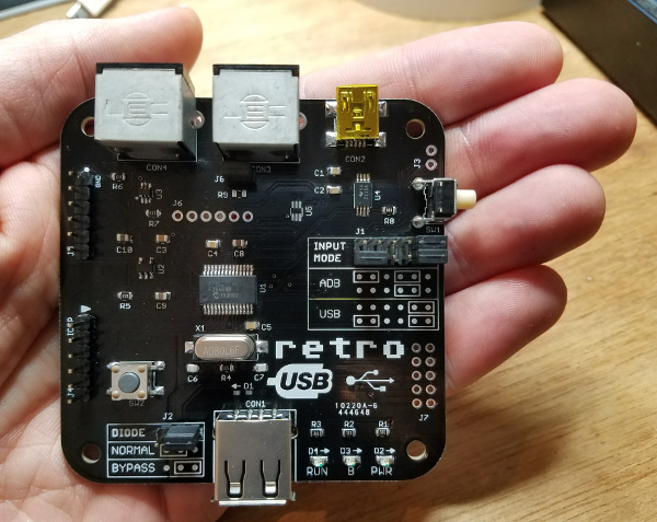
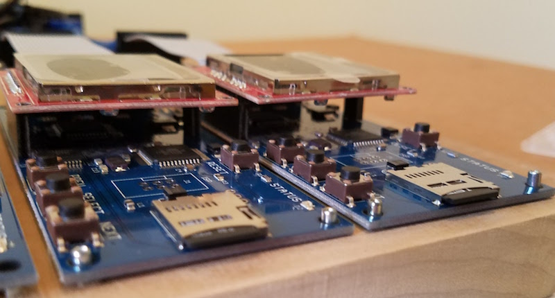
Retro USB boards are here. They look pretty! And they actually work – minus some small fixes I had to apply.
I was in the midst of typing up a description about how my test board didn’t work, and feeling sorry for myself, when I remembered the issue with the external crystal that occurred with the breadboard prototype a few weeks ago. I couldn’t get the crystal to work reliably on the breadboard, so I substituted an external “can oscillator” for testing. That required changing some configuration bits for the PIC32’s clock source – bits that I forgot to change back once I had the real PCB. After I made that change, everything was good.
I’ll be very happy to retire the breadboard, with its delicate wiring that’s thrown off by the smallest bump, and switch over to a nice sturdy PCB for further development. Although within the first 10 minutes of use I already identified a long list of things I want to change about the PCB. For example, I located the serial port and ICSP headers too close to each other, so the PICKit3 programmer blocks the serial port. Doh! And a couple of the components I selected (like U3 in the photo) are way too tiny, and a real pain to solder. SOT-363 sounds fine when it’s some acronym, but perspective changes when you see it’s a 6-pin chip that’s the size of a sesame seed. I had to get a 10x loupe magnifier just to read the markings on the chip. But on the whole, the board seems completely usable, even though it makes some assembly and programming tasks slightly awkward. I think it’s a pretty good first attempt.
Read 9 comments and join the conversationPIC32MX Mini-Review
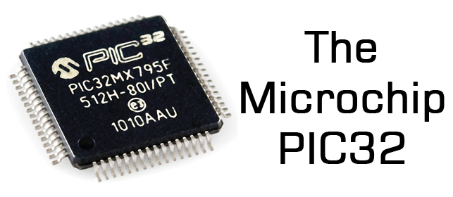
Now that I’ve been using a PIC32MX microcontroller for a while, and its associated software tools from Microchip, it’s time for a mini-review. My previous microcontroller experience was primarily with 8-bit Atmel AVRs, so my comments will reflect that. Many of the differences between a PIC32MX and AVR will also apply to any other modern 32-bit microcontroller, like the many ARM variants.
On the whole, I’ve been fairly pleased with the PIC32MX. Below you’ll see that I’ve written much more about dislikes than likes, but that’s because the likes are largely self-explanatory, while the dislikes deserve a more detailed explanation.
Note: Last year Microchip purchased Atmel, the makers of the AVR. So now both of the microcontrollers in my comparison are provided by the same company.
HARDWARE LIKES
Faster core speeds – Up to 50 MHz on my PIC32MX230F256, 80 MHz on other devices in this family.
Clock PLL – Synthesize core speeds anywhere from 1 MHz to 50 MHz from a fixed-speed external crystal or internal RC oscillator.
More flash memory – 256KB seems like a lot.
Configurable pin remapping – Relocate functions like the UART’s TXD and RXD to one of several different possible physical pin locations. Makes PCB routing much easier.
Set / clear / invert registers – Modify a single GPIO pin with a single instruction, without needing to do a read-modify-write of an entire port.
DMA – I haven’t used it yet, but this will enable possibilities like writing a long piece of text to the serial port while the program continues on to do other things.
SOFTWARE LIKES
IDE – The Microchip MPLAB X IDE seems pretty good, after you install the separate PLIB libraries that are required for compiling all the example code.
Debugger – With the el-cheapo PICKit 3 programming tool, you get a halfway decent debugger in MPLAB X. I can’t believe I survived for years on the AVR with no debugger at all.
HARDWARE DISLIKES
Bloaty code – A similar amount of code seems to consume substantially more program flash memory on the PIC32MX than the AVR, so the larger amount of flash on the device isn’t as much of an advantage as it first seems. Part of this is due to the hardware difference between 8-bit and 32-bit instructions, and part due to compiler optimizations to software (see below).
Awkward bootloader setup – The PIC32MX230F256 has 3KB of protected boot flash, which isn’t enough to do anything useful, considering how bloaty the code is, and that more than 1KB will be consumed by interrupt vector tables and the C startup code. My USB mass storage device bootloader is 39KB of code! This forces the bootloader to be located in main program flash, which requires using a customized linker script for the main program to map everything to new memory locations, which requires that the bootloaded and non-bootloaded versions of the main program are subtly different.
No EEPROM – AVR has separate non-volatile EEPROM memory for storing user preference data, that can be updated one byte at a time, and is rated for 100K erase cycles. PIC32MX has no equivalent. You can reuse some of the program flash memory for the same purpose, but it can only be updated one page at a time (1K or 4K depending on the device) and is rated for 10K erase cycles.
Fewer instructions per clock cycle – AVR executes one instruction per clock cycle, so 16 MHz means 16 MIPS. The number of instructions per clock cycle for PIC32MX varies, but will on average be less than one, due to flash memory wait states, addressing modes, pipeline stalls, and other factors. So while the core speed of PIC32MX might be 3x faster than AVR, it won’t necessarily run code 3x faster.
SOFTWARE DISLIKES
Debugger limitations – When using the PICKit 3, the debugger can’t view arbitrary memory or array elements, can’t set new breakpoints while the program is already running, can’t step through a disassembled view of arbitrary code (without a map file), and is incredibly slow for single-stepping through code. I’m not sure if these are software issues, or limitations of the PICKit 3. Microchip offers other more expensive debugging tools that may address these issues.
Limited compiler optimizations – The XC32 compiler that’s included with MPLAB X will compile your code with -O0 (no optimization) or -O1 (some optimization for speed and size). But it won’t do -O2 (more optimization for speed) or -Os (optimize for size). It also won’t do a bunch of related linker optimizations to help reduce code size. Those require the pro version of the compiler, which is a $30/month subscription.
Mixed quality libraries and code examples – Almost all the PIC example code you’ll find on the web, from Microchip or 3rd parties, uses the PLIB peripheral library along with MLA (Microchip libraries for applications). A few years ago these were officially discontinued in favor of a newer solution called Harmony, but the developer community has largely ignored Harmony and continued using PLIB and MLA. The strong impression I had was that attempting to use Harmony would make life unnecessarily difficult. Yet some of Microchip’s newer code examples are only available in Harmony versions, while older examples are only PLIB/MLA versions, resulting in a confusing mess.
Many of the PIC32MX code examples I found were designed for the top of the line, the PIC32MX795. These examples are mostly applicable to the PIC32MX2xx family too, but sometimes there are subtle differences that are difficult to catch. For example, Microchip’s PIC32 USB mass storage bootloader example assumed the device had a flash erase page size of 4K, with a comment in the code that said “do not change this value”. Only after much frustration did I discover why it wasn’t working reliably – the PIC32MX2xx has a 1K flash erase page, so the Microchip code was only erasing 1/4 of the the flash memory during bootloading.
Read 3 comments and join the conversationElectronic Junk Mail Teardown
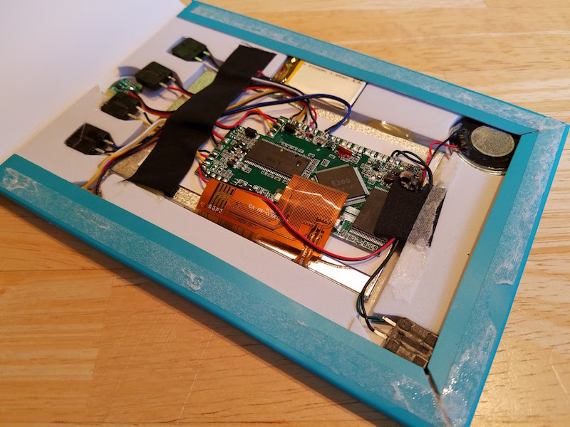
I recently got some very surprising junk mail that contained a full-fledged embedded computer. This was a first for me, but I wonder if there will be more to come? Of course I couldn’t resist the temptation to tear it apart and see what was inside.
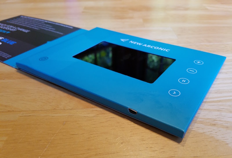
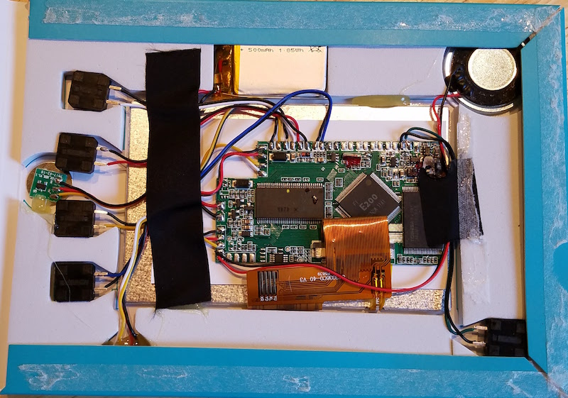
The mail was something related to “The New Arconic”, which appears to be a proxy fight over control of the Arconic corporation (formerly Alcoa, the Aluminum Company of America). They want me to vote for new candidates for the board of directors – blah blah boring. But instead of sending me a persuasive letter or glossy brochure, they mailed a purpose-built video player with a 3 inch TFT screen and control buttons built into a small cardboard envelope.

Nothing happened when I pressed the power button. Dead battery? I located a micro-USB connector on the side, plugged in a charger, and waited. After a few minutes, the distinct aroma of fried electronics began to fill the air, and the cardboard was extremely hot. Doh! Of course, the only thing left to do was tear the paper apart and see what was inside.
The guts contained a TFT display module, with a piece of paper glued to the back, and a small circuit board affixed to the paper. Everything was connected by point-to-point wiring, and appeared to be hand-soldered. A 500 mAh 1.85 Wh LiPo battery powered the system. Five standard 12 mm tactile switches were taped around the edges, and a circular element in the corner I’m guessing was a piezo speaker. The only component I couldn’t identify was a tiny circuit board containing a single 3-pin chip, attached to a 1cm circular metal disk. It’s labeled Q5, and I’m guessing it’s the transistor used to enable power to the main board. [It’s actually a magnetic relay that turns on the power when you open the box cover.]
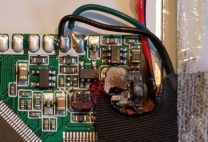
The burnt part of the circuit was clearly identifiable, in a corner of the main board near what looked like two inductors.
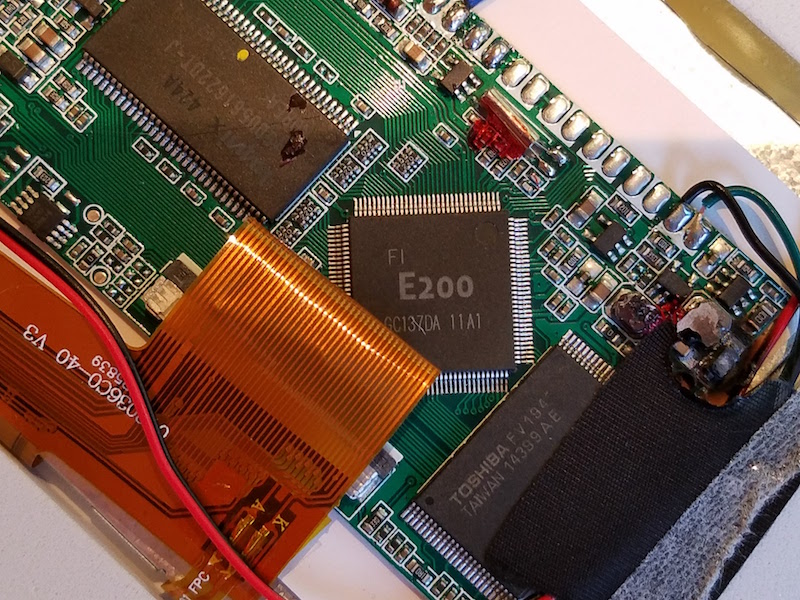
The main board contained three large chips: a Toshiba FV194 14399AE, a Hynix _Y5DU561622DT-J, and an unbranded E200 GC137DA. The first letter of the Hynix part number was obscured by burnt crud. I couldn’t find any info on the Toshiba chip, but based on its appearance and by process of elimination I’m guessing it’s a flash ROM containing the video file to be played. The Hynix part is DRAM of some type, though I couldn’t find an exact match on the part. The E200 is a PowerPC based system-on-a-chip. While searching for info about it, I found this Hackaday article from 2014 describing a teardown of very similar hardware. It looks like this is a standard platform for disposable electronic advertising, and the Italian company that makes them is here.
Given that they mailed me a fire hazard that needs to be specially recycled, I’m not too sympathetic to New Arconic’s advertising.
Retro USB in Reverse
This Retro USB conversion stuff is getting interesting. Last week I showed off my first working prototype of USB to ADB input conversion. After another week of tinkering, I’ve now got the reverse conversion working as well. I can use my early 80’s keyboard and mouse on my 21st century Windows desktop machine! It’s awesome, in a totally useless kind of way.
As entertaining as this is, I’m not sure it makes sense to include this feature in the final Retro USB design. While it’s not conceptually difficult to do the conversion in reverse, it complicates the software and hardware for a feature that’s basically just a novelty. It means a USB-B port would be required, along with some way of switching between it and the USB-A port that’s safe and idiot-proof. It also means the ADB port would either be a source of power, or a peripheral that needs to be supplied power. It’s not a huge problem, but it’s lots of extra fiddly bits to design and include in the hardware. I’m thinking it may be better to keep things simple and focus exclusively on USB-to-ADB, which would help keep the cost down too. Or maybe I could find a way to offer ADB-to-USB as an extra option for those who really want it.
Read 4 comments and join the conversationThe Programming Board
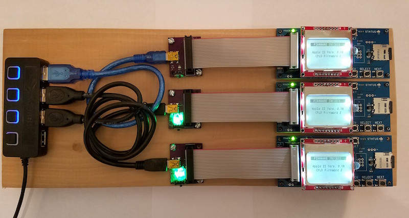
Behold the Floppy Emu programming board! Normally when you read “programming board” on this web site, you’d think of some circuitry on a PCB, but this time it’s a 3/4 inch thick plank of poplar wood. Ah, that kind of programming board!
Sometimes I need to reprogram a large number of Floppy Emus, and this tool makes the job much easier. My old method was to connect the Emus one at a time to an Apple IIgs, turn on the computer, push buttons to begin a firmware update, and then wait ~30 seconds for the update to finish. It was a slow and inconvenient process when dozens or hundreds of Emus needed reprogramming. With the programming board, I can slap down one Floppy Emu into a bracket, start the firmware update going, and then rotate to the next Floppy Emu. Everything is powered from a USB supply, and I use a hub with individual lighted switches to turn on power for each Emu bracket.
Updating three Floppy Emus in parallel is a big improvement, but there’s also another trick here that makes the process even better. With the old method on the IIgs, some fiddling with cables was necessary every time I connected or disconnected a Floppy Emu. Things would slide around on my desk, and I’d waste time getting the connectors lined up. The programming board uses metal pegs at each bracket to hold the Floppy Emu centered, so a short 4-inch ribbon cable can drop down perfectly aligned with the connector every time. Here’s a close-up of the alignment pegs:
If you’re wondering about those green lights on the bottom two power adapters, they’re not status indicators, but just simple power lights. I accidentally bought some high-brightness LEDs, and even with under 10 mA current they’re so bright that it’s irritating. They’re dazzling to the point of being blinding. Fortunately the LED in the top-most power adapter didn’t work due to my lousy soldering job. I covered the bottom two with 5 layers of paper, which cuts down and diffuses the brightness enough to be tolerable.
Read 2 comments and join the conversationReflow Soldering Re-re-re-revisited
This was my 6th *@#&% attempt to assemble some ROM-inator II PCBs using reflow soldering, instead of my normal drag-soldering with an iron. I may not be too bright, but at least I’m persistent. All of the previous attempts failed in slightly different ways, resulting in boards with multiple solder bridges that needed to be cleaned up manually with an iron. This time I altered the way I created a frame for the board being reflowed, and it almost worked. It was certainly the best result so far, but still not good enough.
You can read about the previous reflow attempts here:
1. Reflow with hot air
2. Switched to a hot plate
3. With an aluminum pie pan
4. New solder paste and aluminum sheet
5. Using a stainless steel stencil
My reflow soldering adventures have been a challenge for two reasons:
1. The ROM-inator II PCB has two chips with 0.5mm pin spacing, which is very small. If my boards had larger components with more forgiving pin spacing, my earlier attempts would probably have gone much better. 0.5mm might be approaching the limit of what can be done at home without special equipment.
2. I need the PCB to be 100% perfect after reflow, with no manual touch-ups required to fix solder bridges. If this were a one-off prototype, a few solder bridges would be no big deal. But since my goal is to develop a new process that’s faster than hand-soldering, I can’t afford the time needed to do manual touch-ups after reflow.
Floating Stencils
In my previous attempt, I used purpose-made plastic framing pieces to hold the PCB while I applied solder paste with the stencil. These plastic pieces were a tiny bit thicker than the PCB, resulting in the stencil floating above the surface of the PCB instead of resting on it. The amount of float was less than 0.3 mm, but it was still enough to cause problems. This time I used extra PCBs to create a frame, so the thickness was an exact match with no float. The solder paste application looked pretty much spot-on, as you can see here:
Placement of the chips is still difficult. I’m doing it by hand with a pair of tweezers, and the best I can do is to drop the chip within a couple of millimeters of the correct position. Then I slide it around until it’s in the right spot, smearing a bit of the solder paste in the process. Here’s how things looked after chip placement:
After reflow on my hot plate, the results were pretty good, but unfortunately there were still several solder bridges. Here’s a typical example. It all looks decent, except for those two pins at the far left. The chip also didn’t snap to the correct alignment, as I’d been led to believe would happen thanks to the surface tension of liquid solder. The alignment is pretty good, but not quite centered, and there’s a bridge at pin 1:
I assembled ten boards this way, with two chips per board, and two sides to be soldered per chip, making a total of 40 sides. The good news was that 14 of the 40 sides had zero solder bridges. The bad news was that about half the sides had 2+ solder bridges, and I never assembled a PCB that didn’t have at least one solder bridge on it somewhere. This was the final score:
0 solder bridges: 14 sides
1 solder bridge: 7 sides
2 solder bridges: 7 sides
3 solder bridges: 3 sides
4+ solder bridges: 9 sides
I discovered that I needed to wipe both sides of the stencil clean after each use, otherwise the solder paste application grew progressively messier with each new PCB. I also found that I wasted a lot of solder paste. Dispensing the minimum possible amount from my syringe was still too much, and resulted in a lot of leftover paste on my plastic scraping tool. It was hard to reuse the paste stuck to the scraper. When I tried it a couple of times, using another scraper to clean off the first scraper, the results weren’t good.
End?
Is this the end of my reflow soldering saga? I think so, at least for this particular PCB. I don’t think I can improve further on these results without more effort than can be justified, yet the speed and quality of the process isn’t good enough to replace my current method of drag-soldering with an iron. I’ll revisit this again the next time I have a new PCB to assemble, and I’ll try to stay away from 0.5 mm pitch parts in my designs.
Read 7 comments and join the conversation